PCB Routing Rules: Current Path, Return Path, and Crosstalk
Routing quality decides whether an electronic product performs, survives, and ships on schedule. The same schematic can produce a quiet board or one that resets when a motor starts, and the difference is almost always in the routing. The rules below are the ones that carry the most weight in practice, organised the way an engineer actually applies them: understand the current path, prepare before drawing, then route and check.
The current path comes first
The primary job of routing is to give current an effective path between components. Copper is not free of resistance, and a trace that is too narrow produces a voltage drop that shows up as a supply sag or a signal that no longer reaches its threshold. Shortening the path and choosing the right width are therefore the first two decisions, and they apply to power nets long before they apply to signals.
High-speed signals add three more concerns: reflection, crosstalk, and delay. Those effects distort the waveform and disturb timing, so the routing rules for them are about controlled length and matched impedance rather than about resistance alone.
Electromagnetic compatibility starts at the loop
A changing current creates a magnetic field, and a changing magnetic field induces a voltage in any conductor that shares that field. That single fact explains most coupling problems. Routing that encloses a large area turns into a loop antenna, and a loop that couples into a neighbouring trace turns into crosstalk.
The countermeasures follow directly: avoid large current loops, keep sensitive circuits away from the sources that generate those fields, and provide a return path close to every signal. A continuous ground layer under the trace is the most effective of these, and a shield can or a conductive enclosure handles what the layer cannot.
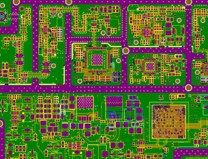
Loops are easiest to see on a drawing of the return path. If the return current has to travel around an obstacle instead of beneath the trace, the loop area has grown and so has the radiation.
Set the rules before the first trace
Design rules belong to the preparation stage. Trace width, spacing, and via size are chosen from the working voltage, current, and frequency of each net. High-current nets get wider copper to reduce resistance; high-frequency nets get shorter runs and no right-angle corners, because the corner is an impedance discontinuity and a source of radiation.
Placement follows the same discipline. Important blocks and the parts that are hardest to place go down first, and the connections that matter most are made as short as the layout allows. High-frequency and low-frequency sections are separated while the floor plan is still fluid, because moving them later costs a re-layout.
Power, ground, and decoupling
Supply and ground nets carry the largest currents on the board, so they get wider copper. A decoupling capacitor belongs at the supply pin of every integrated circuit, connected with the shortest loop the layout allows, because the capacitor only works through the loop it closes with the device.
Ground treatment deserves its own section in the design notes. Analog and digital sections are routed separately, their returns are kept separate, and the two references are joined at one deliberate point rather than everywhere.
Signal routing practice
High-frequency signals are routed as short as possible, and parallel runs between a fast net and a sensitive one are avoided. Where parallelism cannot be avoided, a ground guard line between the two reduces coupling. A trace length that equals an odd multiple of a quarter wavelength at a frequency the circuit cares about will resonate, so those lengths are avoided deliberately rather than by luck.
Direction is the other cheap control. Traces on adjacent layers run in orthogonal directions, which limits layer-to-layer crosstalk, and bends are made with 45 degree segments instead of right angles, which keeps the impedance continuous and limits radiation at the corner. The arithmetic behind spacing rules is covered in our guide to the 3W rule for crosstalk.

A routing review that only checks connectivity misses the two questions that matter: where does the return current flow, and what does this trace run next to.
Details that decide field performance
Four detail checks catch most problems before they reach a prototype. The return loop area is kept as small as the layout allows. Crosstalk is controlled by reducing the distance between the signal layer and its reference plane and by inserting ground guard lines between parallel runs. Clocks and synchronisation signals are treated as critical and given shielding, either as a ground guard or as a coaxial arrangement on the layer. Finally, every stub is checked for a floating end, because an unterminated open trace behaves as a small antenna.
The return path is the thread that connects all four. Our guide to ground routing and power trace planning works through the geometry, and the wider set of suppression techniques is set out in EMI suppression design principles.
Manual routing, automatic routing, and review
Manual routing is still the right choice for critical and high-speed nets, because the path, the width, and the spacing are all engineering decisions. An autorouter is useful for the bulk of ordinary nets, provided the result is reviewed and corrected rather than accepted. Either way, the design rule check is the gate: spacing, width, coupling, and isolated ground sections are verified against the fabrication capability before the data leaves the engineering group.
Optimisation after routing is where a design usually gains its last few points of quality. Teardrops strengthen the junction between a pad and its trace, ground fill fills the unused areas, and moving to a multilayer stackup solves congestion that no amount of trace tuning will fix.
Special signals and edge clearance
Reset, interrupt, and control signals are treated as sensitive nets. They are routed away from the board edge, where they would otherwise pick up noise from cables and handling, and they are kept short. On products that must pass an electrostatic discharge test, devices are placed more than 3.5 mm from the board edge so that a discharge to the edge does not reach the silicon directly.
None of these rules is exotic. What separates a quiet board from a marginal one is that the rules were applied while the layout was still open, and then verified rather than assumed.
Where impedance matching fits
The rules above describe geometry, but the target they serve is electrical. Impedance matching is what keeps a fast edge from reflecting at a transition, and it is specified per net class rather than per trace: a single-ended line is usually controlled at 50 ohm and a differential pair at 100 ohm, with the final values taken from the interface and the stackup. The same set of PCB routing rules then has to be applied consistently along the whole path, because a matched trace that changes width at a via, or that crosses a plane split, is no longer matched.
FAQ
Which rule matters most? The return path. Width, spacing, and corner geometry all matter, but a signal whose return current cannot follow it will radiate and couple regardless of how carefully the trace itself was drawn.
Can an autorouter produce production-quality routing? It can produce usable routing for ordinary nets. Critical nets, clocks, differential pairs, and power paths should be routed manually and reviewed against the rules above.
Why avoid right-angle bends? A right angle changes the trace width electrically at the corner, which produces a local impedance discontinuity and a small radiator. Two 45 degree segments do the same job without either effect.