



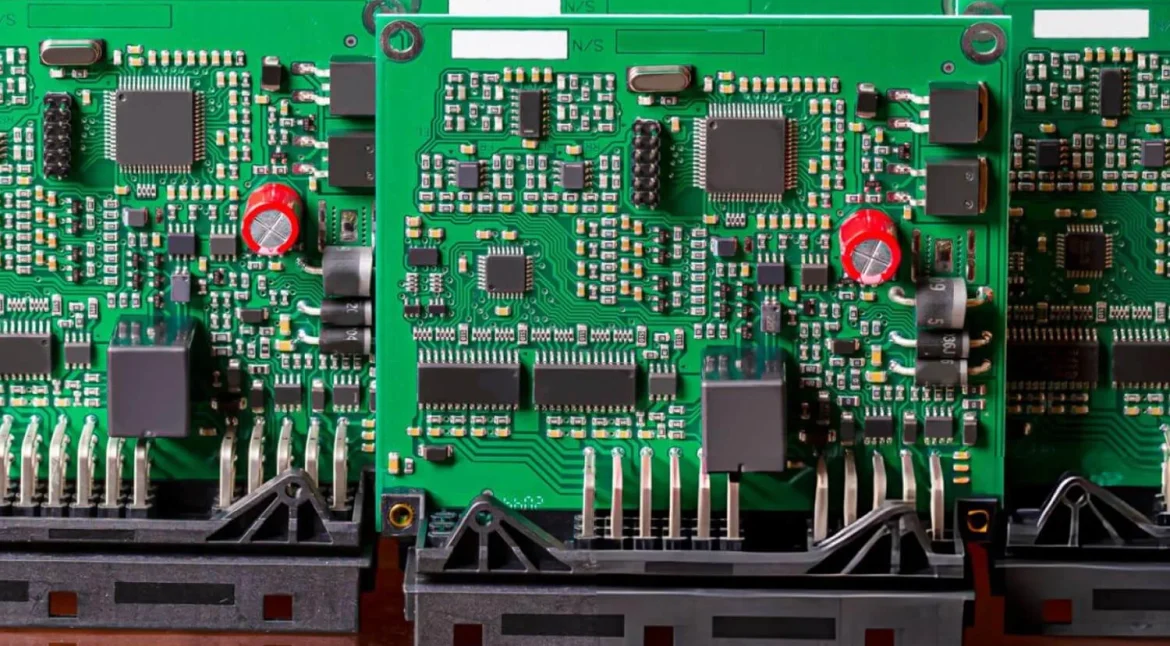
Ground Routing and Power Trace Planning
Routing begins with a decision that is easy to postpone and expensive to revisit: where the ground and the power go. Signal traces are what designers picture when they think about routing, but the ground and power distribution network is what determines whether the signals arrive cleanly. Planning that network before any signal is routed is the difference between a board that behaves as simulated and one that has to be re-spun.
Separation of Analog and Digital Ground
The first planning decision is whether the design needs separate analog and digital ground regions. Where the board contains sensitive analog measurement alongside digital processing, the answer is normally yes. The two regions are routed on separate planes, or on separate regions of one plane, so that the currents that flow in the digital section do not develop voltages in the reference used by the analog section.
The analog ground region is the reference against which every analog measurement is made, so it must be a region that carries no switching current and that has no return path in common with the digital circuitry. An isolation distance of at least 1 mm between the analog and digital regions is the usual starting point. Where the mechanical constraints of a dense board make that impossible, the distance may be reduced, but it should not be reduced casually, because the coupling that the gap controls grows quickly as the spacing shrinks. The physical extent of the separation is a stronger control than any filter placed afterwards.

Flash Copper, Shields and Stitching
Pouring copper over the ground area is one of the cheapest improvements available. A ground pour reduces the resistance and inductance of the return path and gives every trace nearby a reference, which improves both stability and immunity. The benefit is real but conditional: it applies to copper that is connected to ground in a useful way, not to copper that merely exists.
A shield can perform the same function above the board. A metal cover connected to ground at multiple points provides electromagnetic isolation between the circuitry it encloses and the rest of the design, and it also reduces the field that escapes to the outside world. Shields are most effective when the enclosure is connected to ground with a low-inductance path at several points around its perimeter, since a shield grounded at one point behaves as an antenna rather than a barrier.
The pour itself needs to be stitched to the plane below. A regular pattern of ground vias along the edges of the pour and around connectors ties the surface copper to the ground network and prevents the pour from becoming a resonant structure. The techniques for doing this well are described in this article on copper flooding and ground islands.
Removing Slivers, Spikes and Islands
A flooded board inevitably contains copper that serves no purpose. Thin slivers of copper that thread between traces, copper spikes that taper to a point, and isolated islands that no longer connect to the ground network are all common. None of them contribute to shielding, and all of them can affect signal quality.
A copper sliver between two traces does more than look untidy. It changes the effective dielectric environment of both traces, altering their impedance slightly, and it provides a path along which charge can accumulate. Where the sliver is thin enough, it may not survive the etching process uniformly, which makes the local geometry unpredictable. The practical rule is to delete any copper feature that is narrower than the minimum trace width the fabricator can produce reliably.
Islands have a separate failure mode. Copper that is connected to nothing is a floating conductor, and a floating conductor couples to nearby signals and reradiates them. The cure is either to connect the island to ground with a via or to remove it entirely; leaving it in place is the one option that is always wrong.
Power Trace Planning
Power distribution should be planned at the same time as ground, because the two form a pair. Where current is low, a power trace sized for the load and routed with its return nearby is sufficient. Where current is substantial, a power plane is preferable, because the plane offers a cross section that no trace can match in the same footprint. The rules that govern how a power plane is divided and how wide the gaps between nets should be are set out in this discussion of power plane splitting.
Every power trace should be sized for the maximum continuous current plus the transient margin, and the sizing should be checked against both the temperature rise and the voltage drop. A trace that satisfies the temperature criterion may still deliver too low a voltage to a distant load, particularly on a low-voltage core rail where the tolerance is small.
The order in which the traces are routed matters as well. Power and ground should go down first, on the widest practical geometry, because they are the least flexible nets. Signal traces can then be routed in the space that remains, and the designer is not forced into narrow power connections that happen to be the only remaining options.
Bringing the Two Together
Ground routing and power routing meet at the decoupling capacitor. The loop formed by the capacitor, the power pin and the ground plane is what delivers transient current to a switching device, and its area determines how much inductance stands between the capacitor and the load. Keeping that loop small is a placement decision taken before routing begins, and the layout rules that support it are the ones discussed in this article on mixed signal design guidelines.
It is worth noting that the ground network carries the return current of every signal on the board, and the quality of that network therefore sets a ceiling on the signal integrity the design can achieve. A board with a well-planned ground network will outperform a board with better components and a poorer reference, and the difference is visible in measurements long before it is visible on a schematic.
`r`n
A final review should confirm that the analog and digital regions are separated by the intended distance, that every poured region is stitched to ground and free of floating islands, that no copper sliver narrower than the process minimum remains, and that every power path has been sized for both temperature rise and voltage drop.
FAQ
How far apart should analog and digital ground regions be? At least 1 mm as a starting point. The distance may be reduced where the board has no room, but the separation should be treated as the primary isolation mechanism and relaxed only when nothing else is available.
Why is it bad to leave thin copper slivers between traces? Because they alter the dielectric environment of both traces, changing their impedance, and they collect charge. Slivers narrower than the fabricator”s minimum trace width may not etch predictably, which makes the local geometry uncertain.
Should power be routed as a plane or as traces? Use a plane where the current is significant or the voltage drop matters, since a plane provides a far larger cross section for the same footprint. Traces are adequate for low-current rails, provided they are sized for both temperature rise and voltage drop and routed with their returns nearby.


4 Comments
Board Size and Device Placement Practice
[…] Grouping is also what makes the return paths short. When related devices sit together, the return current for their signals flows over a small area of the ground plane, and the loop that could radiate is correspondingly small. The geometry of that return path is the subject of this article on ground routing and power trace planning. […]
Component Placement Guided by the Ratsnest
[…] for each signal depends on where the planes are and how the components are grouped. Sketching the ground and power routing plan while the placement is still fluid often reveals a better grouping than the one on […]
Backplane and Modular Structures in Industrial Control PCB Design - Kingda
[…] The system bus is the interconnection that all modules share, and it behaves differently from a point-to-point connection. Every module connected to the bus presents a load, and every connector and every stub between the bus and the module adds a discontinuity that reflects energy. As modules are added, the loading increases and the reflections accumulate, which is why a bus that works with two cards may fail with six. The countermeasures are to keep the stub from the bus to each module as short as the mechanical design allows, to terminate the bus correctly at the ends, and to define the connector pinout so that each signal is accompanied by a nearby return. Where the bus is fast, the choice between a simple parallel bus and a point-to-point switched fabric becomes a system decision rather than a layout decision. The return structure that makes the bus behave predictably is described in this article on ground routing and power trace planning. […]
Motion Control PCB Design Guide
[…] output close to the device and returning the gate current to the driver ground with a short path. A planned ground and power route drawn before signal routing prevents the loop area from growing as the layout is filled […]