
IC Package Substrate: Structure, Materials and Build-Up Layers
An IC package substrate is the board that carries a bare die and connects its micrometre scale bumps to millimetre scale board pads. It redistributes power, ground and high speed signals, manages heat, and protects the device during assembly. As packages have moved from wire bond to flip chip and from single die to multi-die modules, substrate technology has become one of the limiting factors in semiconductor performance.
What an IC Package Substrate Does
The substrate performs three jobs at once. It fans out the fine pitch of the die to a pitch the motherboard can handle, it delivers power through a low impedance network with enough decoupling to survive fast current transients, and it provides a mechanical body that survives handling, test and reflow.
Electrical performance now sits alongside those functions. High speed interfaces demand controlled impedance traces, low loss dielectrics and short reference paths, and the substrate is often the place where insertion loss is added or saved.
Internal Structure
A typical build-up substrate starts with a rigid core that provides mechanical support and a stable reference plane. Fine line layers are then grown on both faces, connected by laser drilled microvias smaller than 50 µm in diameter. Line and space at the finest layers reaches 8 to 10 µm for advanced flip chip packages, which is far below ordinary PCB capability.
At the top of the stack sit the die pads and the bump landings, and at the bottom the ball pads that connect to the motherboard. The layer count grows with the number of signal pairs, power domains and reference planes that the device needs.
Materials: BT Resin, ABF and Beyond
BT resin, a bismaleimide triazine epoxy, is the workhorse for wire bond and low density flip chip substrates. It is dimensionally stable, has good electrical properties and handles the thermal cycles of assembly without excessive warpage.
ABF, an ajinomoto build-up film, is used for the fine line layers of high performance packages. It supports the very small features required by modern processors at the cost of a more demanding process and a higher price. For RF and millimetre wave devices, low loss materials replace the standard resin to reduce attenuation.
Manufacturing Flow
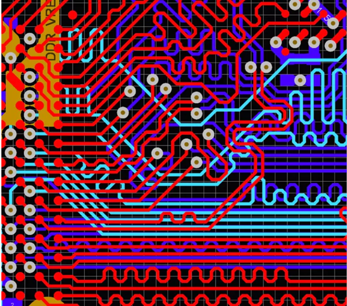
Substrate production follows a build-up HDI sequence at a much finer scale: core drilling and plating, lamination of dielectric films, laser via formation, fine line imaging, plating and repeated build-up until the final layer count is reached. Surface finish and bump pad preparation complete the panel.
Yield management dominates the cost. At line widths below 10 µm, a single defect in a square metre of panel can scrap expensive material, so inspection is performed after every critical step, using automated optical inspection and electrical test on fine pitch probes.
Electrical and Thermal Performance
Signal integrity work on a substrate is similar to high speed board design, but the dimensions are smaller and the loss budget is tighter. Controlled impedance, low skew between a differential pair and a continuous reference plane all have to survive the build-up process. Thermal performance depends on the copper content, the via density under the die and the thermal path into the motherboard.
Mechanical performance is dominated by warpage control. The coefficient of thermal expansion of the substrate has to sit between the die and the motherboard, and the layer stack must be balanced so the package stays flat through reflow. Unbalanced stacks produce warpage that shows up as solder joint defects after assembly.
Substrate Types and Applications
Wire bond substrates use a simpler, coarser build and are cost effective for modest pin counts. Flip chip substrates add a dense bump field and much finer routing. 2.5D and 3D packages place several dies and sometimes memory stacks on one substrate with through silicon vias in the silicon interposer, which pushes line width and layer count to the limit of current capability.
Package on package and system in package modules combine a substrate with embedded components or a second package, and they multiply the routing and warpage challenges again.
Design and Procurement Checklist
When specifying a substrate, state the minimum line and space, the build-up layer count, the core material, the dielectric for each fine layer, the finish on the bump side, the maximum warpage and the thermal cycle requirement. Ask for the actual measured values rather than nominal catalogue data.
Test coverage matters as much as geometry. Fine pitch substrates are normally electrically tested on a dedicated fixture, and the test floor plan should be agreed before tooling, because changing it later means new probes. Data preparation for these builds follows the discipline used in HDI CAM methods and in electroplating and via filling for HDI, with tighter tolerances applied to every step.
Where the Technology Is Heading
Panel level packaging is the main direction of travel. Processing substrates on large panels instead of round wafers lowers cost per unit, but it also demands better registration and cleaning across a large area. Line widths continue to shrink, dielectric loss continues to fall, and the number of dies per package keeps rising.
The practical consequence for buyers is that substrate design has to be planned with the package house and the board fabricator together. A stack that satisfies the die but cannot be assembled onto the motherboard is not a solution, and the review at gopcb covers both ends of that path.
Core Selection and Via Structures
The core sets the mechanical baseline of the package. A thicker core improves rigidity and reduces warpage, while a thin core allows a shorter vertical path and better electrical performance. The choice is usually driven by the package outline: large bodies with a high ball count need more stiffness, and small mobile packages can use a thinner core.
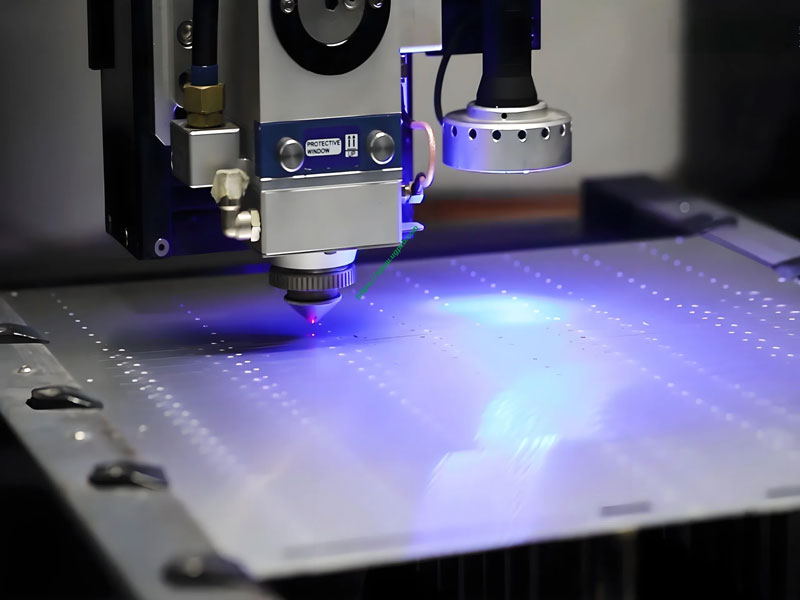
Via structures follow the same logic as a board level design. Microvias connect the fine layers, stacked vias give the shortest path from the die to the ball field, and staggered vias trade a little inductance for a simpler process. The trade-offs between those arrangements are described in the review of blind and buried via stack selection, and they apply unchanged at substrate dimensions.
Core thickness also interacts with the drill schedule. A thin core is easier to drill cleanly but flexes more during handling, so panels are supported on carriers through the fine line steps. Carriers add cost and handling steps, and that trade should be settled with the substrate supplier before the stack is frozen.
FAQ
How is a substrate different from a normal PCB? The process is similar but the scale is not. Line width, via diameter and dielectric thickness are an order of magnitude smaller, and warpage and yield control dominate the engineering effort.
When is ABF used instead of BT resin? ABF is chosen when the fine layers need features below about 15 µm or when the package requires low loss dielectric. BT remains the economical choice for coarser routing and wire bond devices.
Why does substrate warpage matter so much? A warped package will not sit flat on the motherboard, so the ball joints vary in height and some fail during reflow or thermal cycling. Warpage is controlled by balancing the stack and matching expansion to the die and board.