PCB Surface Finish Options Compared
Every copper surface that will be soldered needs a finish, and the choice is made on solderability, flatness, shelf life, and cost rather than on electrical performance. The industry has converged on a small set of options, and each one is the right answer for a specific combination of assembly process and pad geometry. Knowing why each exists makes the selection straightforward instead of a matter of habit.
Hot Air Solder Leveling
Hot air solder leveling, usually called HASL, is the oldest of the common finishes. It coats the copper with solder and then blows the excess off with hot air, leaving a fully wetted, solder-covered surface. Both leaded and lead-free versions exist, and the lead-free variant is the one to specify when the assembly has to comply with lead-free rules.
Its advantages are practical. The copper is completely wetted before assembly, so solderability is predictable; the process is mature and inexpensive; and the finished surface is easy to inspect visually and to probe electrically. Its disadvantage is flatness. The coating thickness varies and the surface is not planar, which makes it a poor choice for fine-pitch surface mount pads or for any land that must be truly coplanar.
Electroless Nickel Immersion Gold
Electroless nickel immersion gold, abbreviated ENIG, is the most widely used finish where flatness matters. A nickel-phosphorus alloy is deposited chemically, and a thin gold layer protects the nickel from oxidation. The phosphorus content of the alloy is itself a process parameter, and the high-phosphorus and medium-phosphorus variants are specified for different applications.
ENIG suits lead-free assembly. Its surface is very flat, which makes it appropriate for fine-pitch placement and for electrical test, and it works for switch and contact designs, wire bonding, and thick boards, while resisting environmental attack well. Its known weakness is the corrosion mechanism the industry calls a black pad, in which the nickel surface is attacked before the gold is deposited and the joint fails at the interface rather than within the solder.
<img src="https://www.gopcba.com/wp-content/uploads/2026/09/24-2.jpg" alt="PCB surface finish comparison across HASL, ENIG and hard gold pads” />
Electroplated Nickel Gold: Hard and Soft
Electroplated nickel gold comes in two forms that behave quite differently. Hard gold, typically a gold-cobalt alloy, is used where the surface will be subjected to mechanical wear, most commonly on edge connectors and gold fingers. Soft gold is essentially pure gold and is used where a wire will be bonded to the surface.
This finish is common on IC substrates, where it serves gold and copper wire bonding. The process has a layout consequence that catches people out: because the gold is deposited by electroplating, the areas to be plated must be electrically connected during the plating step. On a substrate where only the finger region needs gold, a temporary conductive path has to be added to reach it and then removed. The finish is also compatible with electrical test and with contact and switch designs, which is why it persists despite the cost.
Electroless Nickel Electroless Palladium Immersion Gold
Electroless nickel electroless palladium immersion gold, or ENEPIG, adds a palladium layer between the nickel and the gold. It migrated into board fabrication from semiconductor packaging and is now increasingly used on PCB prototypes. The palladium layer is what makes the difference: it separates the gold from the nickel, so the corrosion mechanism that produces a black pad does not occur.
The finish suits both gold and aluminium wire bonding, works with lead-free assembly, and costs less than ENIG or electroplated nickel gold in many cases. It also tolerates being mixed with other finishes on the same board, which matters when a design has regions with different requirements, such as a connector edge that needs wear resistance and a fine-pitch field that needs flatness.
Immersion Silver and Organic Preservatives
Two more finishes deserve a place in the comparison. Immersion silver is chemically simple to apply and is recommended for lead-free assembly and surface mount work, and it is particularly effective on fine features. Its most attractive property is cost: it lowers the overall finishing expense compared with the nickel-gold family, which is why it appears on high-volume boards where the assembly process is well controlled. Its limitation is that silver tarnishes, so the shelf life and the storage conditions matter.
Organic solderability preservatives, usually called OSP, take the opposite approach. Instead of a metal layer, a thin organic film protects the copper and is consumed by the flux during soldering. The surface is flat, the process is simple, and the cost is low. The trade-off is that the protection is fragile: it does not survive repeated reflow cycles well, it is difficult to probe, and the copper underneath is exposed as soon as the film is disturbed.
Choosing by Application
The selection follows from three questions. Does the assembly use lead-free solder, and if so, does the finish have to survive more than one reflow? Does the board have fine-pitch devices that require a flat surface, or lands that need to be coplanar? And will the surface see mechanical wear, as a connector edge does?
A flat, lead-free-compatible finish for fine-pitch work with good shelf life points to one of the nickel-gold options. Immersion silver covers the same flatness need at lower cost when the process is controlled and the parts move quickly. A wear surface points to electroplated hard gold, and a cost-driven design with a short assembly window can live with HASL or OSP. It is also legitimate to specify different finishes on different regions of the same board, since the requirements are regional rather than global. Whichever is chosen, the finish interacts with the solder alloy and the reflow profile, which is why the comparison of lead-free versus leaded solder belongs in the same discussion, along with the plating chemistry described in electroplating additives in PCB.
How the Finish Interacts With the Pad
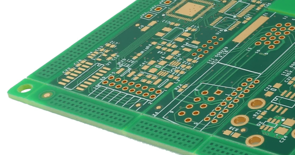
The finish is deposited onto the pad, so the pad geometry governs how well the process behaves. A land with a small annular ring or an irregular shape does not plate or level evenly, and the resulting variation shows up as inconsistent wetting during assembly. For fine-pitch devices, a finish that requires a conductive path for plating adds routing that would not otherwise exist, and that routing has to be removed after plating without damaging the surface. These interactions are the reason a pad geometry review belongs in the same conversation as the finish selection, and the conventions are set out in PCB pad design standards.
There is also a documentation point that saves rework later. Whatever finish is chosen, write it on the fabrication drawing together with the thickness specification and, where relevant, the gold or palladium thickness range. A finish that is left unspecified will be substituted for the cheapest option that satisfies the artwork, and the substitution may not survive the assembly process that the design assumed.
FAQ
Why is HASL a poor choice for fine-pitch parts? Because the coating thickness varies and the surface is not planar, so the pads are not coplanar enough for reliable paste release and placement.
What is a black pad? A corrosion mechanism in ENIG where the nickel surface is attacked before the gold is deposited. The joint then fails at the interface rather than inside the solder.
Why does ENEPIG need a palladium layer? The palladium separates the gold from the nickel, which prevents the corrosion mechanism that causes black pad and makes the finish suitable for both gold and aluminium wire bonding.
Can I use two finishes on one board? Yes. A common combination is hard gold on the connector edge for wear resistance and a flat nickel-gold finish on the fine-pitch field.