Warpage and Fine Lines in an ABF Package Substrate
A package substrate is the board that sits between a semiconductor die and the motherboard, translating a dense array of die pads into a coarser array of solder balls. As dies have grown larger and their connection counts have risen, the substrate has become one of the most demanding pieces of interconnection in the industry, and it is built with a technology that has more in common with semiconductor fabrication than with conventional board manufacturing.
Why a Separate Substrate Is Needed
A modern processor may have thousands of connections at a pitch far below what a motherboard can accept. The substrate fans those connections out, provides the power distribution close to the die, and allows the assembly to be tested and handled as a single component.
It also has to survive the reflow of the die onto it and then the reflow of the whole package onto the board, which is two thermal excursions with different constraints. The mechanical and thermal requirements therefore come from the assembly sequence as much as from the application.
The Build Up Structure
An ABF package substrate is built on a thin core, usually a glass reinforced laminate with a high glass transition temperature. Layers of dielectric film are laminated onto the core, one at a time, and each layer is patterned with fine copper conductors and connected by laser drilled microvias.
The build up approach allows the finest features to be placed in the layers nearest the die, where density is required, while the layers nearer the motherboard use coarser geometry. That gradation is the whole point of the construction, and it is why the layer count can reach twenty or more without the cost of applying fine line rules to every layer.
The Dielectric Film
The film that gives the technology its name is a build up material laminated in thin sheets, cured, and then drilled and plated. Its properties matter in three ways: the dielectric constant and loss affect signal performance, the coefficient of thermal expansion affects warpage and reliability, and the mechanical stiffness affects how thin the package can be made.
The film is also the reason the process works at all. It can be laser drilled with small, clean vias, it adheres to the copper beneath it, and it can be planarised so that the next layer sits on a flat surface. A substrate with twenty layers has nineteen of these film layers stacked, each one planar, and the cumulative flatness is a process achievement rather than a design input.
<img src="https://www.gopcba.com/wp-content/uploads/2026/08/pcb7.jpg" alt="Cross section of a package substrate under a flip chip die” />
Fine Line Formation
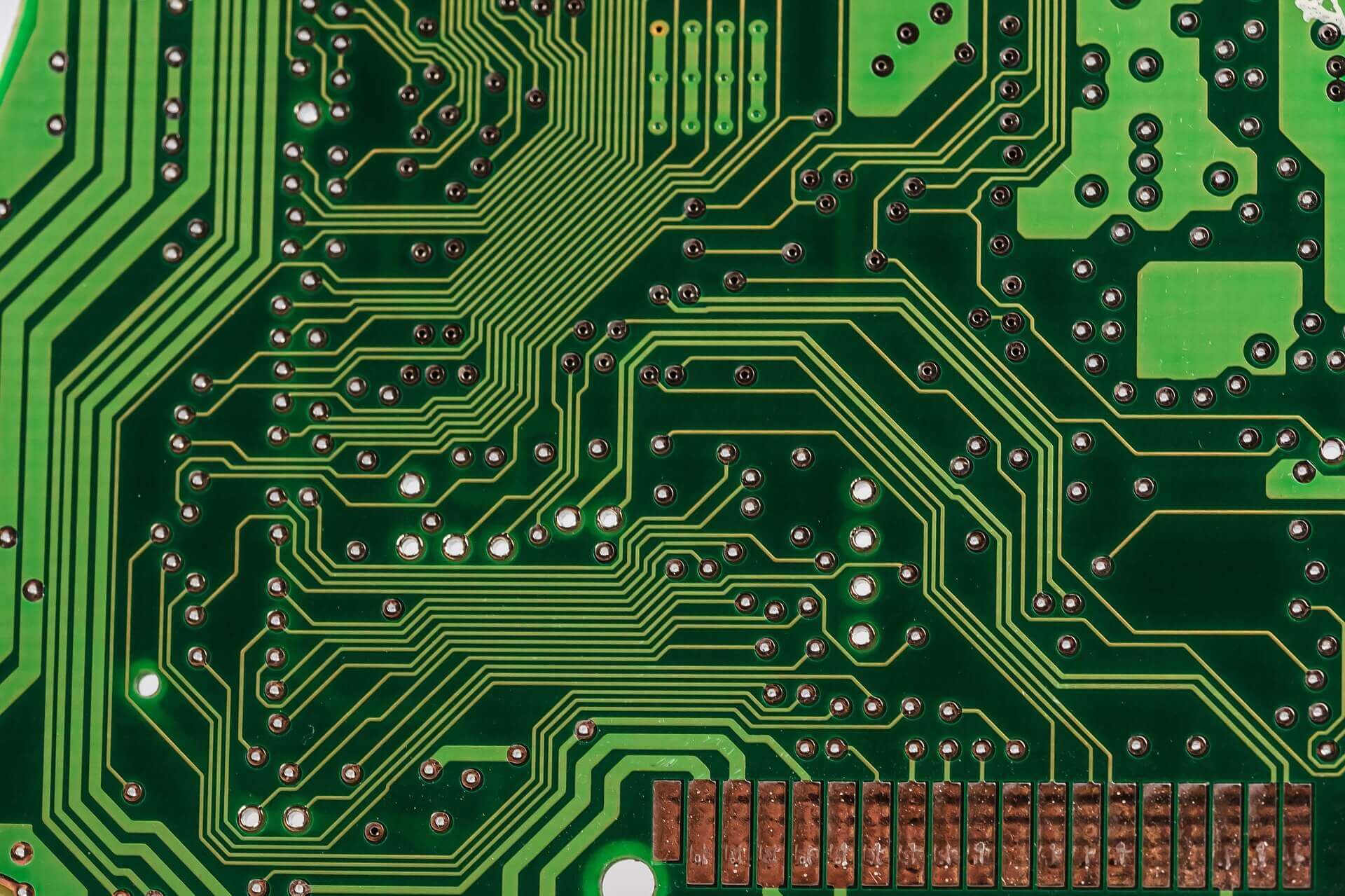
The conductors are formed by a semi-additive process: a thin seed layer, a resist pattern, plating into the openings, and a flash etch to remove the seed between the traces. Because the copper is grown rather than etched away, the traces have a nearly rectangular cross section and the achievable line width is much finer than on a conventional board.
The fine line capability is what allows the escape routing from a dense bump array to be completed in the first layers. Every additional layer adds cost and yield risk, so the design pushes the density into the upper layers and uses relaxed rules lower down. The plating chemistry and its control are the subject of the material on electroplating and via filling.
Microvias and Stacking
Microvias are drilled by laser through a single film layer to connect to the layer below, and they are plated at the same time as the conductors. A via that connects to the layer immediately beneath is the simplest and most reliable form.
Stacked microvias, where a via lands directly on the via below it, allow greater density but concentrate stress along a column, which is a reliability concern under thermal cycling. Staggered vias avoid that concentration at some cost in area, and the trade between the two is the same one described for conventional boards in the discussion of blind and buried via stack selection.
Warpage Control
Warpage is the central challenge of a high layer count substrate. Two different materials are stacked in alternating layers with different expansion coefficients, and the finished part is thin relative to its area, which is the classic recipe for a bowed panel.
Control comes from three directions: a balanced stackup with equal dielectric and copper on either side of the centre, careful control of the copper coverage on each layer, and a lamination process that holds the panel flat. The subsequent thermal excursions of die attach and board assembly then relax or worsen the distortion depending on the design. Warpage that exceeds the specification makes the subsequent assembly impossible, so the flatness limit is a hard constraint rather than a target. The general behaviour of a laminate under thermal load is described in the discussion of a multilayer PCB for high speed.
Power Distribution and Signal Integrity
The substrate has to deliver a large current at a low voltage to the die, with a very small voltage drop, and it has to do so through layers that are also carrying signals. Planes close to the die provide the distributed capacitance that keeps the supply impedance low at high frequency.
Signals travel from the die to the ball array through controlled impedance lines, with lengths matched within a group. The stackup is designed so that the high speed layers have a solid reference on both sides, and the transitions through the build up layers are kept short because a microvia is a discontinuity in an otherwise controlled path.
Applications and Scale
The technology is used for processors, graphics devices, networking chips, high bandwidth memory interfaces and the large programmable devices that sit in data centres. All of them share a large die, a high connection count and a power delivery requirement that a conventional board cannot meet.
Substrate sizes and layer counts have grown steadily, and twenty layers is a routine figure for large devices. The trend towards chiplet architectures, where several dies are mounted on one substrate, increases both the area and the interconnect density, which pushes the technology further in the same direction.
Design and Manufacturing Considerations
Working with this technology requires early involvement of the substrate supplier. The design rules differ from any board design, the tooling lead time is measured in weeks, and the cost of a set of photomasks or a panel tool is significant.
For the assembly, the substrate arrives with its own flatness specification, its own handling requirements and a defined shelf life. Its solder balls are placed and reflowed by a process tuned to the package, and the whole assembly is then tested before it is mounted on the motherboard. Understanding which of those steps constrains the design is the difference between a package that can be built and one that cannot.
FAQ
How does a package substrate differ from an ordinary board? In feature size and in the build up construction. The lines are far finer, the vias are laser drilled through single films, and the layer count and flatness requirements are much tighter.
Why is the core needed at all? It provides mechanical support and dimensional stability during the many lamination cycles, and it carries the coarser routing that connects to the ball array.
Can the design be changed late? Not cheaply. Each layer has its own tooling, and the lead time for a new set is measured in weeks, so the routing should be frozen before the layers are committed.