High Speed Clock PCB Design: Jitter, Impedance and Routing
Every synchronous system has one net that matters more than the rest. The clock sets the instant at which everything else is sampled, so a small error on that net becomes an error everywhere. High speed clock routing is therefore less about raw data rate than about keeping edges clean, keeping timing margins intact and keeping the clock from injecting noise into the rest of the board.
Why a Clock Net Is Not Like Other Nets
A data net carries information that changes from cycle to cycle and can often tolerate a small amount of distortion. A clock net switches continuously at the same rate and is used as a reference by many receivers at once. Errors accumulate rather than averaging out, and the same net is usually the strongest periodic source of emission on the board.
The clock is also the one net that reaches the most places. A single oscillator may drive a processor, a memory controller, several interfaces and a converter, and the distribution network that carries it is a transmission structure in its own right. Treating it as an ordinary trace and hoping for the best is where most signal integrity and timing problems begin.
Rise Time, Not Frequency, Sets the Problem
The frequency on the label is a poor guide to difficulty. What matters is the edge rate, because the harmonic content of a fast edge extends far above the repetition rate. A ten megahertz clock with a sub nanosecond edge has meaningful energy in the high hundreds of megahertz, and at those frequencies a few centimetres of trace behaves as a transmission line with impedance, delay and reflection.
The practical test is the electrical length of the trace compared with the edge. Once the propagation delay of the route approaches a fraction of the rise time, the route must be treated as a transmission line and terminated accordingly. Below that threshold the same route can be treated as a lumped connection, and the design rules relax.

Clock Jitter and Where It Comes From
Clock jitter is the variation of the actual edge position from the ideal one. Some of it is inherent to the oscillator and the phase locked loop and cannot be removed by layout, but a large part is added by the board. Supply noise moves the switching threshold and modulates the delay; crosstalk from neighbouring fast nets shifts the point at which the receiver crosses its threshold; and ground bounce in a shared return path does the same thing on a larger scale.
Because jitter is additive, the layout should be judged by how little it adds. A quiet supply, a solid reference plane, generous separation from switching nodes and a well terminated route all reduce the contribution of the board. Where the requirement is tight, the clock generator should have its own low noise regulator and its own local decoupling rather than sharing a rail with a switching converter.
Impedance Control and the Stackup
Impedance control starts with the stackup. A single ended clock is usually routed as fifty ohms, and a differential clock as one hundred ohms, with the target chosen to match the driver and the receiver rather than copied from a reference design. The geometry that produces the target depends on dielectric thickness and dielectric constant, so the calculation has to use the laminate the fabricator will actually build.
The route should also stay on one layer as far as possible. Changing layers introduces vias, which add capacitance, create stubs and disturb the return path. Where a layer change is unavoidable, place a ground via next to the signal via and keep the reference plane the same on both layers. The structures available are described in microstrip and stripline routing.
Crosstalk and Clock Routing Rules
Because the clock switches at every cycle, it is the most likely aggressor on the board. Long parallel runs beside data lines couple a fraction of the clock into them, and the resulting disturbance can be enough to move a receiver across its threshold at the wrong moment. Separation is the cheapest cure, followed by shorter parallel lengths and by routing the clock on a layer with a close reference plane.
Guard traces are sometimes used, but they only help if they are properly grounded with frequent vias and if they do not disturb the return path they are meant to protect. Where a rule of thumb is used at all, it should be a starting point rather than an answer; the reasoning behind the common spacing rule is explained in the 3W rule and crosstalk control.
Power Integrity and Decoupling
A clock generator draws current in short bursts at each edge, and the supply network has to deliver that current without drooping. The decoupling capacitor at the pin provides the first reservoir, the plane pair provides the second, and the regulator provides the last. Each has a frequency range in which it is effective, which is why a single large capacitor at the pin is not a substitute for a well designed plane and a properly placed regulator.
Ground and power planes also carry the return current of the clock. A plane split under the clock, or a plane stitched with vias that force the return current to detour, raises the impedance of the path and adds noise to the supply. Keeping the reference continuous and keeping the noisy switching currents away from the clock area are more effective than any amount of additional capacitance.
Distributing One Clock to Many Loads
When a clock must reach several receivers, the distribution topology matters. A daisy chain loads each receiver with a stub, which produces reflections that grow with the number of loads. A star or a tree with matched branches and controlled lengths keeps each receiver at the end of its own terminated route, which is preferred as the rate rises.
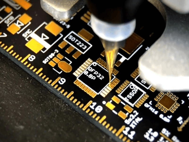
Length matching between branches should follow the setup and hold budget rather than a fixed number, and the matching tolerance should be stated in the same units the fabricator uses for the stackup. Where several clocks must arrive with a defined phase relationship, the skew between the routes is what matters, and the general principles are covered in high frequency trace and data bus routing.
Termination, Materials and Measurement
Termination is part of the clock design, not an afterthought. Series termination at the driver is common for a single point to point route, and parallel or Thevenin termination is used where the driver cannot be placed close to the load. The value should be chosen with the actual trace impedance in mind, and the resistor should be placed as close to the driver as the layout allows.
Material choice follows the length of the route and the rate of the edge. Standard FR4 is adequate for short routes, while longer distribution or lower jitter budgets call for a laminate with lower loss and a more stable dielectric constant. Once the board exists, the clock should be measured at the receiver with a low capacitance probe, because probing the driver pin adds loading that hides the very effect the measurement is meant to reveal.
FAQ
Does a slow clock need impedance control? Only if its edges are fast. A slow clock with a slow edge behaves as a lumped net, but a slow clock with a fast buffer may still need termination and a controlled route.
How much crosstalk is acceptable on a clock net? It depends on the receiver threshold and the jitter budget. The limit is usually a small fraction of the swing, and it should be checked rather than assumed.
Should a clock be routed on an inner layer? Often yes. An inner layer with a close reference plane gives a controlled environment and shields the clock from surface noise, at the cost of vias at each end of the route.