
Impedance Control From Stackup to Routing: A Working Method
Impedance control is often treated as a checkbox: specify fifty ohms, tick the box, and expect the fabricator to deliver it. In practice it is a workflow in which the designer, the fabricator and the measurement instrument each play a part, and the result is only as good as the weakest step. A board can be perfectly built and still fail its impedance requirement because the coupon was measured under different conditions from the specification.
Why Impedance Control Is a Workflow
The target impedance depends on geometry and material, the geometry depends on the stackup, the stackup depends on what the fabricator can build, and the verification depends on how the measurement is defined. Each of those links has to be closed for the finished board to meet the number on the drawing. Skipping one produces a design that looks correct and measures wrong.
The workflow also runs in a specific order. Deciding the impedance target after the stackup is fixed leaves no room to adjust, and deciding the measurement condition after the boards are built makes it impossible to referee a disagreement. Sequence matters more than sophistication.
Step One: Choose the Stackup With the Fabricator
The stackup determines the dielectric heights available, and those heights set the achievable impedance for a given trace width. A common failure is to design a stackup for routing convenience and then discover that the target impedance requires a trace width the design cannot accommodate. The conversation with the fabricator belongs at the start, not at the quotation stage.
Ask about the material options, the available prepreg and core thicknesses, and the copper weights the fabricator uses routinely. Where a specific impedance is critical, a stackup built from standard materials is usually cheaper and more predictable than a custom arrangement, because the fabricator has process data for it already. Our notes on prepreg and core explain the building blocks that the stackup is assembled from.
Step Two: Convert Targets Into Geometry
Once the stackup is fixed, each impedance target becomes a trace geometry: width, and for differential pairs, width and gap. This is normally done with the fabricator’s field solver rather than with a general purpose calculator, because the solver accounts for solder mask, copper thickness and the actual dielectric constants of the chosen materials.
The output should be a table that maps each layer and structure to a width, with the tolerance that the process can hold. That table becomes the design rule the layout has to satisfy, and it is the reference for reviewing the finished artwork. Without it, the layout is guessing.
Step Three: Build the Coupon Into the Panel
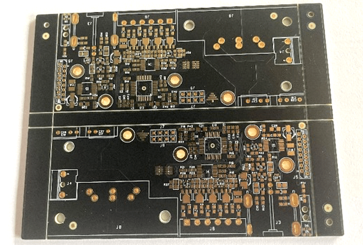
A test coupon is a structure placed on the production panel, not on the product, that replicates the impedance controlled geometry. It allows the fabricator to measure the process without destroying a product board, and it gives the designer a number that describes what was actually built. The coupon should use the same width, the same layer and the same reference spacing as the product.
It should also be measured in the same condition. A coupon measured before solder mask and a product specification that assumes the coated value will disagree by a few percent, and that difference is a measurement artefact rather than a manufacturing defect. Our notes on impedance tolerance describe how to state the condition so that both parties are comparing the same thing.
Step Four: Define the Measurement Condition
The measurement condition includes the instrument, the probe or fixture, the reference plane and the point along the trace where the reading is taken. Time domain reflectometry reports the impedance profile along the trace, so it shows discontinuities as well as the nominal value, and where it is read matters. Averaging over a connector region produces a different number from averaging over the middle of a uniform route.
Writing those details into the specification removes most of the scope for argument later. It also improves the design, because a fabricator who knows exactly how the measurement will be made can advise on the structures that are most sensitive to process variation.
Step Five: Verify and Feed Back
When the panels arrive, the measured coupon data should be compared with the target and with previous lots. A drift over time indicates a process change; a consistent offset indicates a model that needs adjusting. Both are actionable, and both are invisible if the data is filed without being read.
Feedback should reach the library as well. If a particular geometry repeatedly measures low, the rule for that layer should be updated so that the next design starts from a more accurate model rather than repeating the correction. Our outline of layout verification methods treats that loop as part of the design process rather than as a manufacturing concern.
Common Failures in the Workflow
The most frequent problems are familiar. The stackup was fixed before the impedance requirement was known, so the required width does not fit. The rule table was never translated into the design rules, so the layout drifts away from it without anyone noticing. The coupon geometry differs from the product, so the measurement describes a structure nobody is using. Or the tolerance was specified without a measurement condition, which makes acceptance a matter of opinion.
None of these requires advanced analysis to avoid. They require the workflow to be followed in order and the decisions to be written down where the next engineer can find them.
Additional Considerations for This Build
Practical attention to test coupon pays for itself here, because it is one of the items that decides whether the finished board behaves as the drawing intended. Where the requirement is not stated on the fabrication drawing or in the assembly notes, the shop has to assume a default, and that default is rarely the value the design was simulated with. Stating test coupon explicitly, together with the tolerance that applies, removes the assumption and keeps the result predictable from batch to batch.
One more part of the workflow deserves attention: the copper surrounding the trace. A pour, a plane edge, a neighbouring trace or a component pad all change the local impedance, and a design that models only the trace and the plane beneath it will be slightly optimistic. Where the budget is tight, tell the fabricator which areas contain pours or dense copper so the model can account for them, and keep the geometry consistent along a controlled route, because a change in the surrounding copper has the same effect as a change in the trace itself. Treating the environment as part of the structure, rather than as background, is what makes the measured result match the intent rather than something discovered at measurement.
FAQ
Who should calculate the trace geometry? The fabricator, using the materials they will actually use and a field solver that includes solder mask effects. A designer working from a general calculator will usually be a few percent out, and that difference may be the whole tolerance budget.
How many coupons are needed per panel? Enough to represent the variation across the panel, which usually means more than one. A single coupon measured at one point tells you the value at that point, not the value the product will experience across the panel and across the lot.
What if the measured impedance is outside tolerance? First establish that the measurement condition matches the specification, because a mismatch in coupon state or probe position is a common cause of apparent failure. If the measurement is valid, the fabricator can adjust the etch compensation or the geometry, and the corrected stackup should be recorded for the next run.