Stamp Holes and Breakaway Tabs for Small Boards
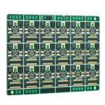
Small boards cannot be assembled one at a time, so they are produced in a panel and separated afterwards. The separation point is designed, not accidental, and the two common ways to design it are a row of small holes and a routed tab. Both work, and both fail in characteristic ways when the surrounding geometry is chosen carelessly.
Why Small Boards Need a Panel
Placement equipment, conveyor rails and reflow ovens are all designed around a minimum panel size. A board of a few centimetres will not transport reliably by itself and cannot be held by the standard tooling, so it is combined with others in a panel that the line can handle, and panel design is the discipline of making that combination work. The panel also allows the assembler to place components once per panel rather than once per board.
The penalty is that the panel has to be broken apart after assembly, and every method of doing that applies mechanical stress close to the finished circuitry. Depaneling is therefore a design problem: the geometry determines where the material breaks, how much energy reaches the board, and what the edge looks like afterwards.
How Stamp Holes Work
A row of small holes along the intended break line creates a perforation. The remaining material between the holes, called the web, holds the board during assembly and breaks when the board is bent or pushed. Because the break is initiated at the holes, it follows the designed line rather than the operator’s judgement.
This is the reason stamp holes are preferred for irregular outlines and for boards where a straight edge is not available. The technique does not require a straight line, and it can follow a curved or stepped contour that a scoring wheel cannot produce.
Hole Pattern and Web Width
The hole diameter, the spacing between holes and the web that remains all determine how easily the board separates and how much damage the separation causes. A wide web holds the board securely but requires more force to break, which propagates stress further into the board. A narrow web separates easily but can break during handling before assembly is complete.
As a starting point, the holes are usually small, spaced so that the remaining web is a fraction of the hole diameter, and arranged so that the perforation is as short as the outline allows. The exact values depend on the board thickness and the laminate, which is why the pattern should be agreed with the fabricator and the assembler rather than chosen from a drawing.
Tab Placement and Routing Keep-Out
Every tab is a piece of material that connects the board to the frame, and every break releases energy. Where a tab meets the board, the copper has to be kept away from the break line by a margin large enough to absorb the crack propagation and the burr that follows it. Traces that run right up to the edge of a break line are the most common cause of a lifted pad or a cracked conductor after depaneling.
Tab positions also matter for assembly. A tab that sits under a large component prevents the board from lying flat, and a tab placed near a connector can obstruct the housing during test. Our notes on board outline and mounting design cover the clearances worth reserving around the outline for each class of hardware.
<img src="https://www.gopcba.com/wp-content/uploads/2026/09/52.webp" alt="Breakaway tab with mouse bites after depaneling” />
V-Score Versus Breakaway Tabs
Scoring cuts a V-shaped groove along a straight edge and leaves a defined web of material that snaps when the board is flexed. It is fast and produces a clean straight edge, but it only works on straight lines, and the groove depth has to be controlled: too shallow and the board will not break cleanly, too deep and the panel may break during assembly.
Stamp holes and routed tabs handle curved outlines and irregular shapes, and they allow the panel to be more densely packed. The choice is usually made on the board outline and on the number of boards in the panel, and a mixed panel using both techniques is entirely normal.
Edge Quality and Burrs
Separation leaves an edge that is never as clean as a routed edge. Small burrs, a slightly ragged contour and a small amount of delamination at the break line are normal consequences of the process, and the design has to tolerate them. Keeping copper and mask back from the break line is the principal protection.
Where the edge will be visible or touched, the acceptance criterion should be set with the customer rather than assumed. A cosmetic burr that is acceptable inside an enclosure may be a rejection on a visible surface, and the difference affects how the panel is designed and how the boards are handled after separation.
Depaneling Methods and Their Effect
Breaking by hand is the least controlled method and applies bending stress through the board. A dedicated depaneling tool, or a router that removes the tab material, applies less stress and produces a more consistent edge. Where the board carries brittle components or a ceramic substrate, the choice of method is often more important than the hole pattern.
The stress imposed during depaneling also depends on how the board is supported. A board with no support under the break line will flex, and the flexure reaches the components rather than the perforation. Supporting the board close to the break line directs the force where it is intended.
Design Rules That Prevent Damage
The rules that matter are about distance. Keep copper, vias and mask openings away from the break line by the margin the process and the laminate require. Keep components, especially brittle ones, out of the region that will flex. Keep the panel balanced so that the boards do not distort during reflow.
Our notes on PCB slot and edge routing rules describe how routed slots and tabs are dimensioned for the same reason, and how the two approaches can be combined in one panel.
Ordering and Communication
Stamp holes, tabs and scoring are all documented by the fabricator rather than by the designer, which makes them easy to get wrong. Showing the intended break line on the fabrication drawing, and stating how the boards will be separated, removes the ambiguity that otherwise produces a panel that cannot be depaneled without damage.
Our notes on PCB area estimation explain how the frame, the tabs and the spacing between boards affect the panel that must be ordered, which is the number that appears in the quotation. At gopcb, the panel layout and the separation method are agreed together so that the delivered panel matches how the boards will actually be built and split.
FAQ
Are stamp holes better than a V-score? Neither is universally better. A score gives a cleaner straight edge and a tighter panel; stamp holes handle curved outlines and irregular shapes where scoring is impossible.
How far should copper be kept from a break line? Far enough to absorb the crack and the burr, which depends on the laminate and the separation method. The fabricator’s recommendation for the specific panel is more reliable than a general rule.
Can a board be broken by hand without damage? Sometimes, if the pattern is designed for it and the board is supported correctly. Where the board carries brittle parts, a controlled depaneling tool is worth the additional processing step.