
Checking Reference Plane Splits Before Release
A reference plane split is one of the few layout defects that is invisible in every standard check and fatal in the finished product. The netlist is correct, the clearance rules are satisfied and the connectivity is complete, yet any signal that crosses the split has no return path directly beneath it and behaves as though its impedance were undefined.
This article explains why splits matter, the difference between the two kinds of split, and how to check for them systematically before a layout is released.
The reason the check is worth automating is that splits appear late, usually when a plane is edited for a reason unrelated to the signals that cross it, and a manual review of a dense board does not reliably find them.
Two Kinds Of Split
A plane can be divided by a deliberate boundary between two different supplies, or by an accumulation of clearances around vias and through holes that ends up cutting the copper in a line. The first is intentional and can be planned for; the second is usually accidental and appears where nobody was looking.
Both produce the same effect on a signal crossing them. The return current cannot follow the trace directly, so it detours around the end of the gap. The detour adds inductance, which raises the impedance of the line at that point and creates a radiating loop whose size is the area enclosed by the detour.

What The Detour Costs
Two costs are incurred. The first is a local impedance discontinuity that reflects part of the signal and consumes timing margin, in the same way as any other discontinuity. The second, and generally the larger, is the common mode current that flows in the detour loop and radiates.
That radiation is why a board can pass a functional test and fail an emissions test without anything obviously wrong. The split forces the return current to take a path that makes the board behave as an unintentional antenna, and the emission is strongest at the frequency whose wavelength matches the loop.
Deliberate Splits Between Supplies
A split between two supply voltages is often necessary, but the placement of the boundary is a design decision. Wherever possible the boundary should run where no signal crosses it, which typically means aligning it with the boundary between two functional regions rather than through the middle of a bus.
Where a signal must cross, the return path has to be restored. A capacitor bridging the two planes provides a path for the high frequency return current, and its effectiveness depends on the inductance of its connection and on the frequency of the signal. For a fast signal the capacitor is usually inadequate, and the better answer is to change the layer assignment so that the signal does not cross. The rules governing how a plane should be divided are set out in the guidance on splitting power planes.
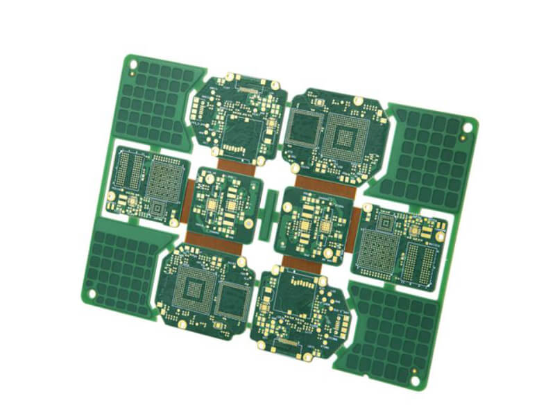
The frequency at which the detour becomes significant depends on the size of the loop it creates and on the edge rate of the signal. A short crossing over a narrow gap produces a small loop and a modest effect, which is why the same split can be harmless on one net and damaging on another routed beside it with a faster driver or a longer parallel section.
Accidental Splits From Clearances
The accidental kind appears in three common ways. A row of via antipads can remove enough copper to form a continuous gap. A dense region of through hole pads can do the same. A region where copper was removed for a mechanical reason, such as a connector cutout or a mounting area, can cut a plane without anybody intending it.
Each of these is easy to find with the right visualisation. The check is to display the plane layer with the clearances visible and look for a line of copper that has been removed across the path of a fast net. Where a gap already exists, adding copper between the clearances or staggering them restores the plane.
Checking Systematically
The practical method is to define the plane nets, then for every high speed net identify the plane it references on each layer it occupies, and check that the referenced plane is continuous along the whole route. Most layout tools can express this as a rule and report the violations.
Where the tool cannot, the check can be approximated by drawing the intended reference region on each layer and comparing it with the actual copper. Both methods rely on the same thing: the reference for a net must be defined explicitly in the design rules rather than assumed. The planning of the ground routing at the start of the layout is what makes the check possible at the end.
Repairing A Split
Where a violation is found, the options are ranked by cost. Moving the signal to another layer avoids the split but adds transitions. Moving the split is usually better if the functional boundary allows it. Adding copper between clearances restores the plane with no electrical change at all, and it is often the cheapest fix.
Where none of these is possible, the remaining option is to shorten the crossing and to accept the discontinuity, documenting the decision. A crossing of a few tenths of a millimetre is far less damaging than one of several millimetres, because the detour loop is smaller. The general rules for controlling coupling between nets also apply to the repair.
Differential pairs are affected differently, and often worse. If one member of a pair crosses a split and the other does not, the two lines see different return paths, the pair becomes unbalanced, and a significant part of the differential signal is converted into common mode. This is one of the few mechanisms that can make a well matched pair radiate, and it is worth checking explicitly whenever a pair changes layer or passes near a plane boundary.
What The Review Should Ask
The first checklist item worth asking directly in a review is which nets cross a plane boundary and what the return path is. The answer should be a short list, and every item on it should have a documented reason. A list that nobody can produce indicates that the question has not been examined.
The second question is whether the plane under each of the board’s power regions has been checked for accidental gaps. Both questions take minutes in a review and can be answered with the layout open, and both prevent the class of problem that is most expensive to find after the board is built.
Finally, the check should be repeated after every significant edit. A plane is usually modified late, for thermal or mechanical reasons, by an engineer who is not thinking about the signals above it. Running the reference check again before release is a two minute operation that catches the change.
FAQ
Do slow signals need to worry about splits? Less, because the return current has more alternatives and the loop radiates less at low frequency. But a slow signal with a fast edge is still a fast signal for this purpose, so the check should be based on the edge rate rather than on the clock.
Can stitching capacitors fix any split? They help below the frequency where the capacitor and its mounting are effective, which is usually a few hundred megahertz. Above that, the return path must be copper.
Is a split ever beneficial? A deliberate split can isolate noisy digital return currents from a sensitive analogue reference, provided that no signal crosses it. The benefit comes from the placement of the boundary rather than from the split itself.