Decoupling Capacitor Placement in HDI Boards with BGA Packages
Decoupling capacitor placement used to be a routine task. The designer put a small capacitor next to every power pin, tied it to the ground plane with a short via, and moved on. In a modern high density interconnect board carrying a large ball grid array, that routine no longer works, because there is no surface area left close enough to the pins to be useful and the vias needed to reach the planes add inductance that swamps the benefit of the part itself.
The consequence is that decoupling has become a power delivery network problem rather than a placement problem. The capacitor is only one element in a chain that includes the package, the balls, the vias, the planes and the regulator. Getting the impedance below the target across the frequency band the device needs is now the design objective, and placement is one of several levers available to reach it.
Why Placement Became the Bottleneck
Ball grid array pitches below 0.8 mm leave no room between balls for a capacitor, and the region directly beneath the package is filled with escape vias. The plane area that used to be available for mounting parts is now occupied by the fanout of the device itself. At the same time the current drawn by the device has risen and the tolerable ripple has fallen, so the capacitor has to be closer and more effective than before, not merely equivalent.
There is also a geometric conflict between density and inductance. A capacitor placed far from the pin sees a long trace and a long via path, and both add inductance in series with the capacitor. Above roughly ten megahertz the inductive reactance of that path dominates the capacitive reactance of the part, so a distant capacitor does nothing useful. The routing that solves the signal escape problem therefore creates the power integrity problem, which is why power plane design and layout have to be planned together rather than in sequence.
The Real Limit Is Loop Inductance
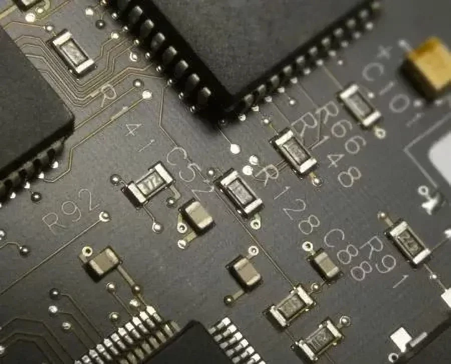
The parameter that decides whether a capacitor works is the loop area enclosed by the current as it leaves the plane through the capacitor and returns to the plane. That loop includes the capacitor body, both pads, both vias and the separation between the power plane and the ground plane. Reducing the dielectric thickness between the planes shrinks the loop and therefore reduces the inductance, which is why a thin core is often more valuable than an additional capacitor.
Coupling the planes with a spacing of four mils or less also provides distributed capacitance that is effective at high frequency, where the planes behave as a transmission line rather than as a lumped element. When that distributed capacitance is present, the exact position of individual capacitors matters much less, because the planes themselves supply the charge at the frequencies where placement would otherwise be critical.
Microvias, Via in Pad and Planar Capacitance
Placing capacitors on the opposite side of the board directly under the device is the standard answer when the component side is full. The capacitor is mounted on the back, and its vias rise through the core to the planes beneath the device. This minimises loop length and avoids sharing the escape region with signal vias. The approach depends on blind or buried vias, which is why via plugging and filling capability becomes a relevant question during board selection.
Via in pad with conductive fill and copper capping is the logical extension. The capacitor sits directly over the via that connects it to the plane, removing the short trace that would otherwise be shared with other parts. The trade off is process cost and a stricter flatness requirement on the pad, since the component must reflow onto a surface that has been filled and plated rather than laminated.
What to Do When the Surface Is Exhausted
When every available site has been used, the next step is to reconsider the package rather than the board. A device with more power pins, a different ball map or a larger body may give back the area that has been lost. Equally, a capacitor in a smaller case size placed closer is usually worth more than a larger capacitor placed further away, even though the larger part has a higher nominal capacitance, because the inductance of the path decides the useful frequency range.
Symmetry is the other tool. Placing capacitors symmetrically around or beneath a device with multiple power pins balances the current that each pin supplies, which reduces the effective inductance seen at the pin and lowers the radiated field from the package. Designs that ignore symmetry often show a resonance in the impedance profile that no amount of extra capacitance removes, because the problem is the mounting rather than the part. Groups of parts that share a rail should also be checked for anti-resonance between the bulk and the high frequency capacitors, which the regulator loop can excite if the damping is inadequate.
Embedded Capacitance and a Three Tier Strategy
Embedded capacitance puts the function inside the stack rather than on the surface. A thin high permittivity layer laminated between a power and a ground plane acts as a distributed capacitor, and because it is located at the plane level the loop inductance is close to zero. The benefit is not only electrical; it also frees surface area for parts that must be mounted, which is exactly the constraint that HDI designs run into.
The most robust approach treats decoupling as three tiers rather than one. Bulk capacitors handle the low frequency content, embedded or planar capacitance covers the middle band, and the on die capacitance of the device handles the very high frequencies that no board level part can reach. Each tier covers the band the others cannot, and the target impedance is met by the sum of the three rather than by any one of them. A dc to dc converter layout that keeps the regulator close and its loop tight then completes the picture at the source end.
Simulation and Verification
Impedance analysis before the placement is frozen is worth far more than analysis afterwards, because a change of stack-up or plane spacing is cheap at that stage and expensive later. The simulation should sweep frequency, include the package model, and report the impedance seen at the device pins against the target curve rather than at the capacitor pads. Results that look acceptable at the capacitor and unacceptable at the pin usually indicate a mounting inductance problem.
After layout, the same model can be re-run with extracted parasitics to confirm that the intended loop inductance was achieved. Measured confirmation is possible with a vector network analyser and a suitable probe, or with a dedicated power integrity fixture, and the measurement is most useful when it is compared against the simulated prediction for the same node. That comparison is what turns a simulation exercise into a design method.
FAQ
How close does a decoupling capacitor need to be? Close enough that the inductance of the mounting path does not dominate the impedance at the highest frequency of interest. In practice that means directly beneath the device or immediately beside the pin group, not at the far end of the rail.
Do more capacitors always help? No. Adding parts with the same mounting inductance in parallel lowers the impedance only until the parallel resonance between them and the planes dominates, and beyond that point the extra parts can make the profile worse.
Is embedded capacitance a replacement for surface capacitors? It replaces the mid frequency parts and reduces the number of surface parts needed, but bulk capacitance is still required for load transients that the thin layer cannot supply.