HDI Boards For Energy Storage Systems: A Selection Guide
Energy storage systems are unusual in that they combine three demands that normally pull a design in different directions: high frequency communication, large currents, and a service life measured in decades outdoors. A battery management controller has to sample cells continuously, report upward over a fast link, and do it inside a cabinet whose volume is shared with power conversion hardware. HDI boards are often the only practical way to fit that capability into the space available.
This article explains what an energy storage application asks of a high density interconnect board, how the stackup and the microvia structure are chosen to answer those demands, and which material and process questions are worth settling before the design is released to fabrication.
Why Energy Storage Needs HDI Boards
The controller of a battery management system has more connections than its enclosure has room for. Cell voltage sense lines, temperature sense lines, isolation barriers, a communication interface and a microcontroller all have to be packed into a module that sits beside the cells. HDI boards answer this with finer traces, smaller vias and more routing layers in the same footprint, so interconnect density rises without making the module larger.
The gain is not density alone. Short traces with a continuous reference plane behind them keep the fast communication link clean, and the same stackup can carry the current of the measurement and balancing circuits on separate copper. A conventional board can be made to work, but it usually needs more layers, a larger area, or both.
Electrical Performance And Impedance Control
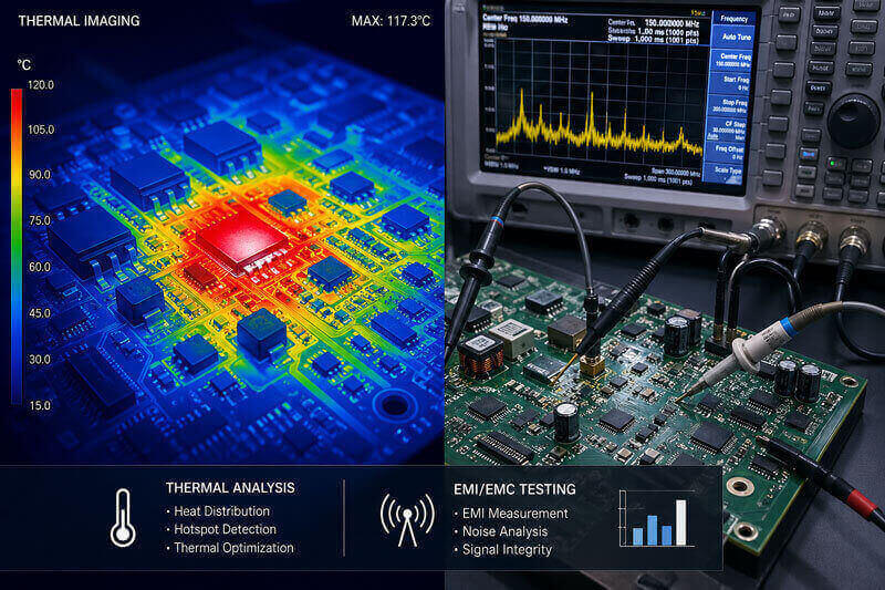
A battery management system samples cells and reports upward, and that reporting link is often a differential or high speed bus. It needs a controlled characteristic impedance, typically held within a few percent, and it needs a dielectric that does not lose much energy at the frequencies involved. Standard FR-4 attenuates more than a high frequency laminate at the top of that range, which is why material choice and impedance control are decided together.
The two numbers that matter are the dielectric constant and the loss factor. A lower dielectric constant lets a wider trace reach the same impedance, which helps both loss and tolerance, while a low loss factor reduces attenuation per unit length. A laminate formulated for high frequency work costs more than FR-4, so it is usually applied to the layers that carry the fast link rather than to the whole stackup. Careful review of the artwork before release confirms that the impedance targets survive the final edits.
Stackup, Microvia Structure And Space
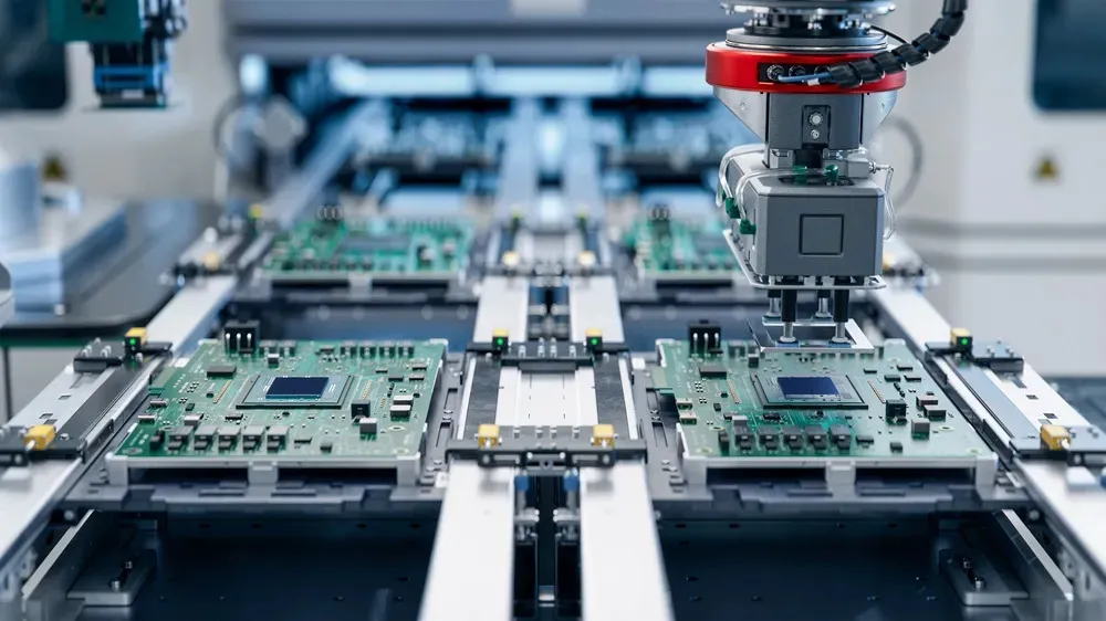
HDI construction builds up thin layers of dielectric with microvia connections between them, drilled by laser rather than mechanically. Because a microvia is small, it can land on a pad and be filled and plated over, which frees the area directly above it for routing. That is what allows a dense device to be placed on a board that would otherwise need many more layers.
The stackup has to balance several things at once: enough layers for the signal and power nets, a reference plane close to the fast traces, and a build up that the fabricator can process reliably. The number and type of blind and buried via structures drives yield and cost, so the stackup should be chosen with the fabricator rather than assumed at the start of layout.
Current, Heat And Thermal Management
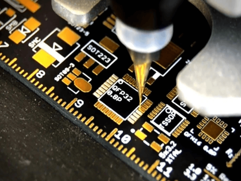
An energy storage board is not only a signal board. Balancing currents, contactor drive and measurement returns all flow through copper on the same substrate, and the copper that carries them dissipates heat. Copper thickness, trace width and layer assignment therefore determine both voltage drop and temperature rise, and the calculation should be done early rather than discovered during a thermal test.
Thermal management uses several routes. The copper itself spreads heat, vias under hot devices carry heat into inner layers, and where a large amount of power has to leave the board, a metal backed or ceramic substrate is used instead of a laminate. Adequate copper and a short thermal path are the two levers, and sizing traces for current is the first step in getting them right.
Reliability Over A Long Service Life
A storage installation is expected to run for a decade or more, and the electronics inside it sees temperature cycling, humidity and, in some locations, salt air. The board has to survive all of it without a field failure, which turns reliability questions into manufacturing questions. Conductor spacing for the working voltage, insulation resistance, and the way a via is filled and capped all affect how long the board lasts.
Microvias deserve particular attention. A plated microvia that is not fully filled can trap chemistry or plate thin in the barrel, and a microvia stacked directly on another is the most demanding case. Filling and plating specifications, plus the acceptance criteria the fabricator applies, are what keep that risk manageable. Industry standards for rigid boards describe the tests that verify the result.
Selecting Material And Process
Selection follows the circuit rather than a catalogue. A board that carries only low frequency measurement and control can stay with FR-4 and standard construction. A board with a high speed link needs a low loss laminate on the relevant layers, controlled impedance and a stackup that keeps the reference plane intact. A board that dissipates significant power needs thicker copper, more vias, or a different substrate.
Once the material is fixed, the process questions follow: minimum line width and spacing, microvia diameter and aspect ratio, the number of lamination cycles, and the surface finish. Each of those is a capability question, and the answer differs from one fabricator to another. The right time to ask is during layout, while the features can still be moved at no cost.
Working With A Fabricator
An energy storage design benefits from a fabricator who has built similar boards. Someone who has processed thin dielectric builds and large copper weights will spot a stackup that is hard to yield before it is ordered, and can suggest an alternative that meets the same electrical requirement at lower cost. That conversation is most useful when it happens with a draft stackup and a net list rather than with finished artwork.
gopcb builds high density and high frequency boards for industrial and energy applications, including multilayer HDI stackups with controlled impedance and heavy copper layers. Reviewing the stackup early, and agreeing the acceptance criteria for microvias up front, removes most of the surprises from the build.
FAQ
Can a standard FR-4 board handle energy storage electronics? For a low frequency control board, yes. Where a high speed link or a tight impedance specification is involved, a low loss laminate or a mixed stackup is the more reliable choice.
How many layers does an energy storage HDI board need? It depends on routing density and on the number of supply nets. Density usually pushes the count up, and each additional lamination cycle adds cost, so the stackup is a compromise rather than a target.
What has to be settled before release? The stackup, the impedance targets, the microvia fill specification and the copper weights for the power nets. Those four items cause most of the rework when they are left open.