Wave Soldering: Process Control for Through-Hole Assemblies
Wave soldering remains the fastest way to attach a large number of through-hole parts, and it remains a process that punishes a board designed without it in mind. The defects it produces are predictable, and almost all of them trace back to a design or a setup decision made long before the board reached the wave.
What the Process Does to the Board
The assembly passes over a fluxer, through a preheat zone and then across a standing wave of molten solder. The wave contacts the underside of the board, fills the plated holes by capillary action and forms fillets on the top side.
Each of those stages depends on the one before it. Flux that is applied unevenly leaves an area that will not wet. Preheat that is too low leaves the flux wet and volatile, producing spatter and voids. Preheat that is too high consumes the flux before the board reaches the wave.
The process is therefore controlled as a sequence, and a defect is best diagnosed by asking which stage failed rather than by adjusting the solder pot temperature, which is the usual first reflex.
Thermal Relief and Copper Loading
A pad connected directly to a plane conducts heat away from the joint far faster than the wave can supply it, and the result is an incomplete fillet on the top side. The standard remedy is a thermal relief, in which the pad is connected to the plane by a small number of narrow spokes rather than by a solid connection.
The number and width of the spokes are a balance. Too much copper and the joint does not reach temperature; too little and the pad is mechanically weak and the plane connection is poor for electrical and thermal purposes.
Copper loading also affects the preheat requirement. A board with heavy plane copper needs more preheat energy to reach the same surface temperature, and the difference is enough that a design change can invalidate a previously tuned profile.
Pad and Hole Geometry
The hole must be large enough for the lead to enter and small enough that capillary action fills the barrel reliably. A hole that is too large allows solder to flow through and form a dome on the top side, which is cosmetically poor and mechanically weak.
Where the lead is a press fit or a square pin, the clearance is tighter and the flow is more reliable. Where the lead is round and small in a large hole, the flow depends almost entirely on the preheat and the flux.
Pad shape matters for bridging. A pad that is round on a fine pitch leaves more space between adjacent pads than an elongated pad, and that space is what keeps a bridge from forming. Our solder defects and board failures notes describe how bridging appears and what causes it.
Orientation and Shadowing
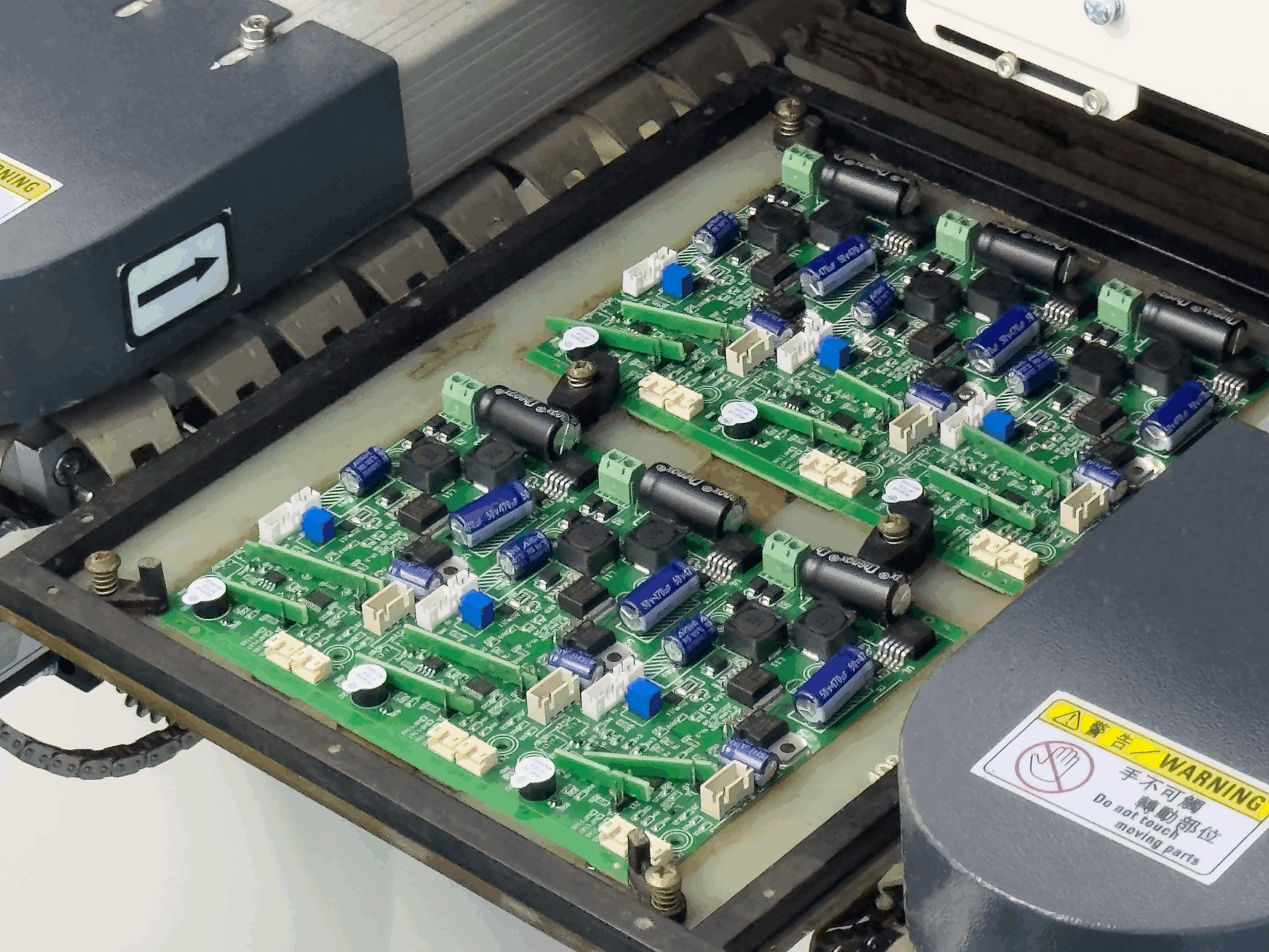
The wave travels in one direction, so a connector body can shield the joints behind it from contact with the solder. The orientation of the part on the board relative to the wave direction determines whether that happens.
The usual convention is to orient long parts perpendicular to the wave so that the solder reaches all the joints at once, and to keep large parts downstream of the small ones. Where the layout does not permit this, the process can sometimes compensate by increasing the wave contact time or using a second wave.
Parts that sit low to the board, such as sockets and connectors with a wide base, are the ones that shadow most. Where their placement is fixed by the mechanical design, the assembly may need selective soldering rather than a wave.
<img src="https://www.gopcba.com/wp-content/uploads/2026/05/工业通信网关PCBA.png" alt="Sectioned through-hole joint showing barrel fill” />
Flux, Residue and Cleaning
Flux chemistry determines whether the assembly will need cleaning and whether the residue will be acceptable. A no-clean flux leaves a residue that is designed to be harmless, but the design assumption is that the residue is thin, evenly distributed and not in contact with moisture.
A water wash flux leaves residue that must be removed, and the removal requires access. A board with parts that trap water, such as connectors with open cavities or components mounted close to the board, may not dry completely after washing.
Our solderability test notes describe how the finish and the flux interact, which is the combination that decides whether a joint forms at all.
Common Defects and Their Causes
Icicles and bridges come from insufficient flux activity, low preheat or excessive contact time. A cold joint with a dull, grainy appearance comes from insufficient heat or from contamination at the surface.
Voids in the fillet usually come from flux volatiles trapped in the barrel as the solder rises, which points at preheat and at flux application rather than at the solder alloy. Solder balls and spatter come from flux that was still wet when the board contacted the wave, which again points at preheat.
Insufficient fill, where the barrel is not filled to the specified height, is usually a hole geometry problem or a preheat problem rather than a solder problem. Measuring the fill on a sectioned sample is the way to distinguish them.
Designing for the Process
Keep the through-hole pad sizes consistent across the board, so that one profile suits all of them. Where a minority of joints need a different treatment, consider whether they can be hand soldered or selectively soldered and excluded from the wave.
Leave enough clearance around each pad for the solder to form a fillet without touching a neighbouring joint, and avoid placing a via in the pad, which allows solder to escape away from the joint.
Place the through-hole parts so that their bodies do not shield each other, and where a large part must be present, orient it so that the shadow falls outside the board or over an area with no joints. Our thermal design notes cover the related question of how copper distribution affects the heating of the assembly.
Verifying the Result
The acceptance criteria for a through-hole joint specify the fillet shape, the fill height in the barrel and the wetting angle on the top side. The criteria are visual, which means the inspection is fast and the training is the limiting factor.
A section through a representative joint confirms the barrel fill and reveals internal voids that the surface appearance does not show. Sectioning one joint per lot is a small cost for the confidence it provides.
Our surface finish notes describe how the finish on the pad influences wetting and how its condition changes with storage, since a finish that has oxidised will not wet regardless of how the wave is set up.
FAQ
Can a surface mount assembly be wave soldered? Parts can be glued and wave soldered from below, but the process is less common now. Where it is used, the parts must be selected for resistance to immersion and the pads shaped to avoid bridging.
Is nitrogen necessary for wave soldering? It improves wetting and reduces dross, and it costs money. It is most valuable on boards with small features and low activity flux.
What does gopcb provide for a wave soldered assembly? We provide pad and thermal relief recommendations matched to the profile, panel and pallet design, sectioned samples to verify barrel fill, and process records for flux, preheat and contact time. Where a design cannot be wave soldered reliably, we say so and propose selective soldering instead.