Plane Capacitance and Embedded Capacitance Materials
A pair of copper planes separated by a thin dielectric is a capacitor distributed across the whole board. It is not a substitute for discrete capacitors, and it does something the discrete parts cannot: it works at the frequencies where their inductance makes them useless.
What a Plane Pair Provides
Two planes carrying power and ground form a capacitor whose value is proportional to the area, the dielectric constant and inversely proportional to the separation. A thin dielectric therefore gives a useful value over a large area.
The capacitance is distributed, so there is no lead inductance between the capacitor and the load. This is the property that makes it effective above a few hundred megahertz where a discrete capacitor’s mounting inductance dominates its performance.
The plane pair also acts as a transmission line, and its impedance at a given frequency is what determines the residual noise. That impedance depends on the plane separation and on the dielectric properties as much as on the capacitance. Our power integrity notes describe how the plane impedance is evaluated.
The Limits of Plane Capacitance
The capacitance available from a plane pair is small compared with a discrete capacitor, typically measured in nanofarads per square centimetre for a conventional stack.
Its value is proportional to the area, so it falls where the planes are interrupted by splits, slots and large numbers of antipads. A plane that is heavily perforated by via holes loses much of its capacitance.
The dielectric between the planes is chosen for its electrical properties rather than for its capacitance, and a low loss material with a low dielectric constant gives less capacitance than a high dielectric constant material. The two requirements pull in opposite directions. Our laminate properties notes describe the trade.
Embedded Capacitance Materials
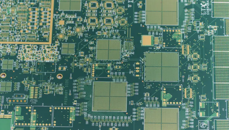
A thin, high dielectric constant layer laminated into the stack provides far more capacitance per unit area than a conventional plane pair. The layer is typically a filled polymer a few tens of micrometres thick.
The material is placed between a power plane and an adjacent ground plane, and it functions as a decoupling layer over the whole area it covers.
The benefit is largest where a large current must be supplied across a broad area at high frequency, such as under a large package or a set of high speed interfaces. Our high frequency laminate notes describe the materials available for the other layers.
Decoupling Strategy and Where Planes Fit
Decoupling is a sequence of capacitors, each covering a frequency range where the previous one has become ineffective. The bulk capacitor covers the low frequencies, the ceramic parts cover the middle, and the plane capacitance and the package cover the high end.
The sequence means that a plane pair is not a replacement for the discrete capacitors. Removing them because the planes provide capacitance leaves the middle of the frequency range uncovered.
The plane pair’s contribution is at the top of the range, where the discrete capacitor’s inductance makes it ineffective. Its value there is set by the plane impedance rather than by a capacitance figure.
Design Measures That Preserve the Plane
Keep the plane continuous under the areas where the current is highest. Splits and slots raise the impedance and reduce the capacitance exactly where it is needed.
Use thin dielectric between the power and ground planes. The separation is the strongest lever available in a conventional stack, and it is a fabrication cost rather than a design complexity.
Where the design requires a split in a plane, provide stitching capacitors across the split at the points where current must cross, so that the high frequency path is not interrupted.
Verification
The verification is a measurement of the plane impedance against frequency, using a network analyzer with a probe or a two port measurement on a test structure.
The measurement shows the resonances of the plane pair, which occur where the plane dimensions correspond to a half wavelength. These resonances are the frequencies at which the plane impedance rises and the decoupling fails.
Where a resonance falls in a band of interest, the remedies are to damp it with a lossy component, to move it by changing the plane dimensions, or to add discrete capacitors at the resonance frequency. Our board design notes describe how the plane dimensions are fixed by the mechanical layout.
When It Is Worth the Cost
An embedded capacitance layer adds material and process cost, and it changes the stack-up. It is justified where the power delivery requirement at high frequency cannot be met with discrete parts, which is usually a large, fast device on a board with limited space for capacitors.
Thinning the dielectric between existing planes is nearly free by comparison and provides a real improvement. It should be considered before an embedded material is specified.
Where the design has plenty of room for capacitors and the currents are modest, the plane pair’s conventional contribution is adequate and no extra steps are needed.
Process Control and Verification
On a design of this kind, dielectric is the item that decides how the rest of the board is arranged. A short note on the drawing about handling, storage or packaging is often worth more than an extra decimal place on a tolerance. Where a value sits close to a process limit, the drawing should say so, since the shop can then open the process window rather than working to a nominal figure that carries no tolerance.
A stack-up that is drawn rather than described removes most of the ambiguity from a quotation, and it lets the fabricator price the board against the dielectric and copper weights that will actually be used. Where the requirement is not written down, the shop supplies its own default, and the default is chosen for the process rather than for the design.
Process Control and Verification
On a design of this kind, dielectric is the item that decides how the rest of the board is arranged. A short note on the drawing about handling, storage or packaging is often worth more than an extra decimal place on a tolerance. Where a value sits close to a process limit, the drawing should say so, since the shop can then open the process window rather than working to a nominal figure that carries no tolerance.
A stack-up that is drawn rather than described removes most of the ambiguity from a quotation, and it lets the fabricator price the board against the dielectric and copper weights that will actually be used.
Process Control and Verification
On a design of this kind, dielectric is the item that decides how the rest of the board is arranged. A short note on the drawing about handling, storage or packaging is often worth more than an extra decimal place on a tolerance. Where a value sits close to a process limit, the drawing should say so, since the shop can then open the process window rather than working to a nominal figure that carries no tolerance.
FAQ
Can plane capacitance replace decoupling capacitors? No. It covers the high frequency end of the range where capacitors are ineffective, and it does not replace their contribution at lower frequencies.
How much capacitance does a plane pair give? A fraction of a nanofarad per square centimetre for a conventional stack, and an order of magnitude more for a thin high dielectric constant layer.
What does gopcb provide for plane capacitance designs? We provide stack-ups with thin power and ground separations, embedded capacitance material options with their process implications, plane impedance measurement on coupons and assemblies, and damping recommendations where a plane resonance falls in a band of interest.