
Capacitor Package Sizes And SMT Process Compatibility
Choosing a capacitor package is often treated as a question of size alone, but the package also has to survive the placement and soldering process that the board will go through. A part that is electrically correct can still cause defects if its dimensional tolerance is loose, if its termination finish wets poorly, or if the reflow profile it needs conflicts with the rest of the assembly. The package is a process decision as much as a layout decision.
This article walks through the common chip sizes, the demands that SMT placement puts on them, and the process windows that matter on a production line. The aim is to make the trade between density and manufacturability explicit, so that a package choice is made deliberately rather than inherited from the last design.
How The Common Capacitor Package Sizes Compare
The 0402 body measures roughly 1.0 by 0.5 millimetres and is the workhorse for dense digital boards, decoupling close to a processor pin where loop inductance matters more than capacitance. The 0805 body, about 2.0 by 1.25 millimetres, is easier to place and inspect, which makes it a reasonable default for industrial and power boards where the layout has room to spare. Neither size is better in the abstract; they serve different constraints.
Larger bodies appear where voltage or capacitance forces them. The 1206 and 1210 sizes carry more ripple current and dissipate more heat, and they are common in supply filtering. Above that, 1812 and 2225 parts appear in high voltage and high capacitance positions. The trend is consistent: as the body grows, the pad area grows, and the amount of solder needed to form a reliable joint grows with it.
What SMT Placement Demands From A Package
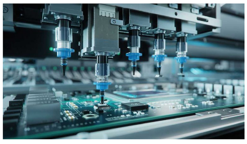
A placement machine holds the part with a nozzle, moves it to a programmed position, and releases it onto the paste. Everything in that sequence depends on the package being consistent. If the length varies across a reel, the nozzle centre will not match the pad centre and the part will sit offset. A placement tolerance of plus or minus 0.05 millimetres looks generous until it is compared with the pad width on a 0402 footprint.
The same logic applies to the height of the termination. A part whose ends are not coplanar with the body will rock on the paste, and rocking is the beginning of a tombstone defect. Suppliers control this with the dimensional tolerance quoted on the datasheet, which is why that figure deserves attention during part selection rather than being accepted without reading it.
Dimensional Tolerance And Pad Geometry
Industry standards set the length and width tolerance of a chip capacitor at plus or minus 0.1 millimetres for most sizes, and the footprint on the board is usually designed around the nominal dimension plus an allowance. If the footprint is drawn tight to the nominal, a part at the upper end of the tolerance will not self align during reflow. If it is drawn too wide, the part can rotate before the solder solidifies.
The practical rule is to keep the gap between the pads equal to the nominal body length, and to extend each pad outward by an amount that gives the solder fillet somewhere to form. For a 0402 part that extension is small, often 0.2 to 0.3 millimetres, while a 1206 part tolerates a wider fillet. Getting this wrong is one of the most common reasons that a design works on a prototype line and struggles in volume.
Reflow Profile And Thermal Shock
A lead free process reaches a peak of about 260 degrees Celsius with a tolerance of five degrees, and a leaded process reaches about 235 degrees. The capacitor sees that peak for a short time, but it also sees the ramp rate, and a fast ramp puts a thermal gradient across the ceramic body. Multilayer ceramics are brittle, and a gradient that is steep enough will produce a microcrack that passes electrical test and fails later.
The reflow profile should therefore be checked against the part rating and not only against the paste datasheet. Many suppliers publish a maximum ramp rate and a number of tolerated cycles, and boards that go through a second reflow for a second side should be evaluated against that cycle count. A part rated for three reflows and run through five is being used outside its specification.
Wettability And Termination Finish
Wettability describes how readily molten solder spreads across the termination, and it depends on the finish. Nickel barrier terminations with a tin overcoat are the common choice and wet reliably in both leaded and lead free processes. Silver palladium and gold finishes appear where a specific compatibility is required, but each has its own storage life and its own sensitivity to contamination.
Poor wettability shows up as a joint that forms a ball rather than a fillet, or as a termination that is only partly covered. Both reduce the mechanical strength of the joint and increase its resistance. If a batch of parts wets poorly, check the storage conditions first: humidity and age affect the finish, and a reel that has been open for a long period may need a bake before use.
Choosing A Package For A New Design
Start from the electrical requirement and then narrow by process. A decoupling position that needs a low inductance path argues for the smallest body that the assembly house can place reliably, while a bulk position argues for a larger body with a better ripple current rating. The size that is correct is the one that satisfies both the electrical and the process constraints, and that is rarely the smallest part available.
It is worth confirming the choice with the assembly partner before the layout is frozen. Placement machine capability, stencil aperture limits and inspection resolution all vary between lines, and a package that one factory runs comfortably may be difficult at another. A short conversation at the layout stage is cheaper than a redesign after the first production run.
Process Control and Verification
On a design of this kind, reflow profile is the item that decides how the rest of the board is arranged. Keeping a sample from the panel turns a dispute into a measurement, because the same coupon can be re-examined by both parties without rebuilding the batch. Reviewing the design before the data is released is cheaper than correcting it after the panel is in the tank, because every step downstream inherits the decision made at the front end.
Related reading: our fabrication notes, board quality and design release notes cover the same ground.
FAQ
Is a smaller capacitor package always better for high speed decoupling? It usually has lower parasitic inductance, but the gain is lost if the part cannot be placed accurately or if the via to the plane adds more inductance than the body saves.
Can a 0402 part be replaced with an 0805 on the same footprint? Only if the footprint is redrawn. The pad gap and the fillet allowance differ, and forcing a larger body onto a small footprint produces a joint that is mechanically weak.
Does the termination finish affect the reflow profile? It affects how the solder wets rather than the temperature that is needed, but a poorly wetting finish may need more time above liquidus, which in turn loads the ceramic body thermally.