3D Printed PCB Prototyping: What It Can Do
Printing a circuit instead of etching one has moved from a laboratory demonstration to a practical prototyping method for some applications. The technology works, but its resolution, materials and electrical behaviour differ from a conventional board in ways that decide where it can be used.
How Conductive Printing Works
A printer deposits a conductive material, usually a metal loaded ink or paste, onto a substrate in the pattern of the conductors. The deposit is then cured or sintered to raise its conductivity towards that of bulk metal.
Sintering is the limiting step for most machines. The particles have to be joined without damaging the substrate, which is why the process works well on polyimide and poorly on a material that cannot take the temperature the ink requires.
What the Process Is Good At
Prototyping is where printing fits today. A design can be turned into a functional board in hours and a revision can be printed the same day, which is far quicker than ordering a fabricated board and waiting for delivery.
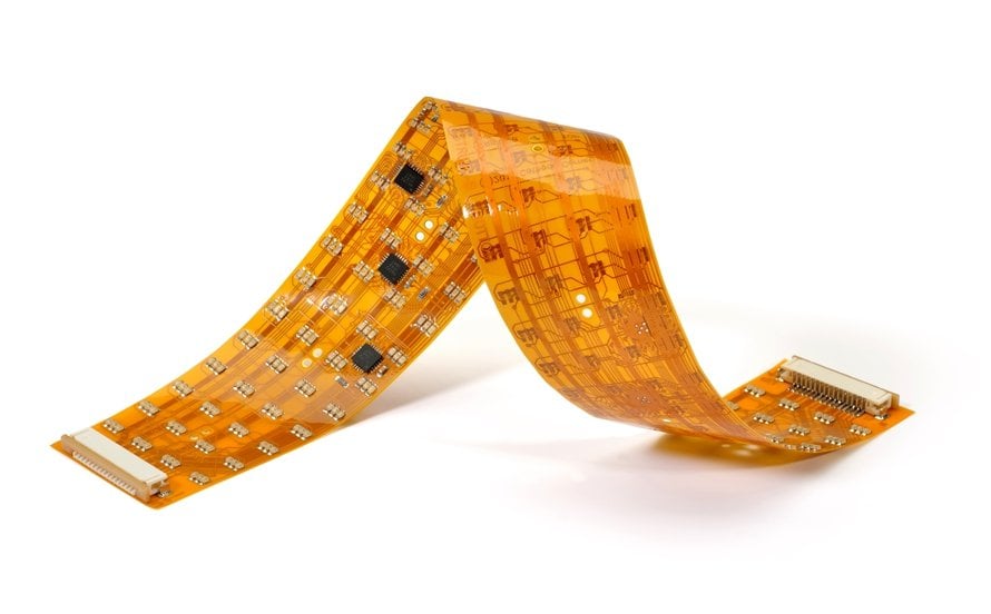
It also suits unusual shapes. A conductor printed onto a curved housing, or into a slot that no laminate could occupy, is a genuine advantage, and the tooling cost is close to zero because there is no tooling to make.

Resolution and Conductivity Limits
The resolution of a printed conductor is measured in tens or hundreds of micrometres, one to two orders of magnitude coarser than a fabricated board. Fine pitch packages and impedance controlled traces are therefore out of reach.
Conductivity is the second limit. A sintered ink has a higher resistivity than rolled copper, so a printed trace of the same width carries less current and dissipates more heat, and the design has to allow for both effects.
Liquid and Flexible Structures
Research into printing within liquids has produced three dimensional channels with micrometre scale diameters, formed by injecting one liquid into another and stabilising the interface with particles. The resulting structures are flexible and can be stretched.
Those channels are interesting for sensors and for flexible circuits rather than for conventional wiring, because the conductor is a liquid and the geometry is a tube rather than a trace. It is a direction of research, not a production process.
Where the Process Does Not Fit
A multilayer board with plated vias, controlled impedance and a solder mask is not something a printer produces today. The plated through hole has no printed equivalent, and without it the routing is limited to one or two layers.
Assembly is a further constraint. A printed conductor has to survive the reflow profile, and the surface has to be compatible with the paste and the finish that the assembly process assumes when it is planned.
<img src="https://www.gopcba.com/wp-content/uploads/2026/06/ISO13485.jpg" alt="Sintered conductive ink test pattern on a printed circuit prototype” />
Choosing Between Printing and Fabrication
The decision usually comes down to time against quality. A printed board is faster and cheaper for the first article, while a fabricated board is the only option for anything that has to go into production or be tested against a specification.
A useful rule is to print the board that proves the circuit and to fabricate the board that proves the product. The two steps answer different questions, and the printing step shortens the loop between them.
Designing for Print
A design intended for printing should keep conductors wide, spacing generous and the number of layers small. Component pads should be dimensioned for the accuracy the printer can hold rather than for a standard land pattern.
Thermal relief becomes more important, because the substrate conducts heat poorly and a pad joined to a large printed plane is difficult to solder. Connectors are best avoided, since their anchors depend on the mechanical strength of the board. The usual prototype file checklist still applies to the data package.
Materials and Curing
Silver inks give the highest conductivity at the highest cost, copper inks need a reducing atmosphere during sintering, and carbon inks are cheap but resistive. The choice follows from the current the trace has to carry and from the environment.
Curing has to be controlled as carefully as printing. An under-cured ink stays resistive and can be removed by later processing, while an over-cured one cracks and loses adhesion, particularly where the board is flexed in service.
Cost and Turnaround
For a single board the printing route can be cheaper than fabrication, because there is no tooling and no shipping time. As quantity rises the advantage disappears, since the printing time per board does not fall in the way that a fabricated panel does.
The comparison should include assembly cost. A printed board that cannot be assembled with the standard process carries a hidden cost that the material price does not show, and that cost usually decides the question.
Where the Technology Is Heading
Machine resolution, ink chemistry and sintering methods are all improving, and the gap between printed and fabricated conductors narrows every year. What has not changed is the physics of a plated via or the tolerance of a controlled impedance trace.
For a designer, the practical position is to watch the technology for the applications where it fits, and to keep the design rules that a fabrication house needs. The prototype cost factors that apply to a fabricated board still apply when a printed board has to be turned into a product.
Process Control and Verification
On a design of this kind, conductive ink is the item that decides how the rest of the board is arranged. The process window is set by the narrowest step in the flow, so an improvement anywhere else shows up as margin rather than as yield until that step is addressed. A short note on the drawing about handling, storage or packaging is often worth more than an extra decimal place on a tolerance.
Process Control and Verification
On a design of this kind, conductive ink is the item that decides how the rest of the board is arranged. The process window is set by the narrowest step in the flow, so an improvement anywhere else shows up as margin rather than as yield until that step is addressed. A short note on the drawing about handling, storage or packaging is often worth more than an extra decimal place on a tolerance.
Where a value sits close to a process limit, the drawing should say so, since the shop can then open the process window rather than working to a nominal figure that carries no tolerance.
Process Control and Verification
On a design of this kind, conductive ink is the item that decides how the rest of the board is arranged. The process window is set by the narrowest step in the flow, so an improvement anywhere else shows up as margin rather than as yield until that step is addressed. A short note on the drawing about handling, storage or packaging is often worth more than an extra decimal place on a tolerance.
FAQ
Can a 3D printed PCB replace a fabricated board? Not for production. Printing suits prototypes, unusual shapes and low current circuits, while fabrication remains necessary for fine pitch, multilayer and impedance controlled designs.
What limits the resolution? The nozzle and the ink, together with the sintering step. Conductors of tens of micrometres can be printed, but not with the yield and repeatability a production board requires.
Is a printed conductor as good as copper? No. Its resistivity is higher, so the same trace carries less current and runs warmer, and the design has to be dimensioned for that.