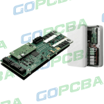
Embedded Busbar Technology in High Current Multilayer PCB Design and Lamination
In high-power electronic systems such as electric vehicle on-board chargers, energy storage converters, server power modules, and industrial inverters, continuous operating current often reaches more than 100 A, and peak current even exceeds 300 A. Traditional PCB design relies on thickened copper foil such as 6 oz, 8 oz, or even 12 oz, or parallel routing to carry high current. However, it faces significant limitations. Thick copper etching becomes extremely difficult, and side etching causes loss of control over line width tolerance. Joule heat accumulation under high current causes local temperature rise to exceed the limit, with delta T greater than 40 degrees Celsius, accelerating copper-resin interface delamination. It also cannot effectively suppress voltage drop, or IR drop, and dynamic voltage drop, or di/dt induced voltage. Embedded busbar technology embeds high-purity electrolytic copper with purity of 99.95 percent or more, in prefabricated thin sheets usually 0.3 to 2.0 mm thick, into the internal dielectric layers of multilayer PCB. Without increasing board thickness, it achieves a current carrying capacity increase of 3 to 5 times, a DC resistance reduction of more than 70 percent, and significantly improves heat diffusion paths and EMI performance.

Key Parameters of Structural Design and Material Selection
Embedded busbar is not simply thickened copper. Its structure requires collaborative consideration of mechanical interlocking, thermal expansion matching, and electrochemical compatibility. The busbar base material should preferably use oxygen-free copper C10200 or phosphorus deoxidized copper C12200, with tensile strength of 205 MPa or more and elongation of 25 percent or more, ensuring resistance to shear deformation during lamination. The busbar surface must undergo micro etching and passivation treatment, such as a benzotriazole BTA passivation layer with thickness of 5 to 10 nm, to suppress copper ion migration to adjacent prepreg during high-temperature lamination and prevent Cu2+ from catalyzing premature aging of epoxy resin. The dielectric layer must use modified epoxy or polyimide-based prepreg with low CTE of 40 ppm per degree Celsius or less and high Tg of 180 degrees Celsius or more, such as ISOLA IS410 or Rogers RO4450F. Its Z-axis coefficient of thermal expansion, or CTE, needs to be as close as possible to that of the busbar at 17 ppm per degree Celsius, avoiding interface peeling stress during temperature cycling. In a typical stack-up, the busbar is covered with a layer of 1080 or 2116 specification prepreg on both top and bottom, with thickness controlled at 0.12 to 0.18 mm, ensuring sufficient resin flow to fill microgaps at the busbar edge and eliminate void risk.
Precision Machining and Positioning Process Control
Busbar prefabricated parts need to be formed by precision stamping or laser cutting, with dimensional tolerance strictly controlled within plus or minus 0.05 mm. The key challenge lies in the interlayer alignment precision between the busbar and the PCB inner layer pattern. If the X or Y direction offset exceeds plus or minus 0.15 mm, it will cause subsequent drilling offset, blind via connection failure, or poor edge solder wicking. The mainstream industry solution uses double-sided optical fiducial marks plus a high-resolution CCD automatic alignment system with repeatability of plus or minus 2 micrometers or less, completing vacuum adsorption bonding of the busbar and core board before lamination. The busbar edge must be designed with a resin relief groove of 0.2 to 0.3 mm width and about 0.05 mm depth to accommodate excess resin flow during lamination, preventing the busbar from being pushed up or prepreg from accumulating at the edge to form stress concentration points. In a certain 8-layer new energy main control board case, a 0.8 mm thick busbar was embedded in layers L4 and L5. By optimizing the resin relief groove structure, the busbar flatness after lamination was maintained within plus or minus 15 micrometers, far better than the plus or minus 65 micrometers of a design without grooves.

Vacuum Hot Pressing Process Window Optimization
Embedded busbar lamination differs from conventional multilayer boards. Its core lies in gradient heating and staged pressure strategy. A typical process curve is divided into four stages. First, preheating stage from room temperature to 100 degrees Celsius at a rate of 1.5 degrees Celsius per minute, allowing prepreg to initially soften and release moisture. Second, medium temperature stage from 100 to 150 degrees Celsius at a rate of 0.8 degrees Celsius per minute, where prepreg viscosity drops to 10 to the 3rd power to 10 to the 4th power Pa seconds, initiating initial pressure of 3 to 5 kgf per square centimeter to promote resin wetting of the busbar side. Third, high temperature curing stage from 150 to 185 degrees Celsius at a rate of 0.5 degrees Celsius per minute, holding at 180 degrees Celsius for 120 minutes and applying final pressure of 15 to 20 kgf per square centimeter, ensuring bonding strength between the busbar and prepreg interface of more than 1.2 N per mm per IPC-TM-650 2.4.9 standard. Fourth, cooling stage from 185 to 80 degrees Celsius at a rate of 1.0 degree Celsius per minute or less, avoiding sudden cooling that causes busbar warping. Measurements show that if the heating rate is too fast, greater than 1.2 degrees Celsius per minute, it is easy to form a resin shadow area at the bottom of the busbar, causing local bonding strength decrease. Insufficient final pressure leads to interface void rate greater than 0.8 percent, significantly deteriorating thermal resistance with R theta JC increased by 35 percent.
Electrical Performance Verification and Reliability Enhancement
The electrical advantages of embedded busbar need to be verified through standardized testing. DC resistance is measured by the four-wire method, or Kelvin sensing, requiring voltage drop of 5 mV per 10 cm or less under 100 A steady-state current, corresponding to a busbar cross-sectional area of 100 square mm or more. Dynamic performance is evaluated by pulse testing. Apply a 500 A per 1 ms square wave current and use a high-frequency current probe with bandwidth of 500 MHz or more to monitor the induced voltage caused by di/dt. The acceptance standard is less than 150 mV, based on L equals dV divided by di times dt to calculate parasitic inductance, with a target value of less than 15 nanohenries. To improve long-term reliability, three key assessments must be performed. First, thermal shock testing from minus 40 to 125 degrees Celsius for 1,000 cycles to inspect copper-prepreg interface delamination. Second, pressure cooker testing at 121 degrees Celsius, 100 percent RH, 2 atm, for 96 hours to verify no electrochemical migration at the busbar edge under humid and hot environments. Third, power cycling testing with 100 A switching, delta T of 80 degrees Celsius, for 10,000 cycles to monitor intermetallic compound growth thickness at the busbar pad, which should be less than 3 micrometers. Mass production batch data from a certain customer shows that busbars with Ni and Au surface treatment plus edge chamfering of R0.15 mm had IMC thickness stable at 1.8 to 2.2 micrometers after power cycling, meeting IEC 60068-2-69 standard requirements.
Comprehensive Comparison with Traditional Thick Copper and External Copper Sheet Solutions
Compared with 6 oz etched thick copper boards, embedded busbar achieves a current density increase of 4.2 times at the same cross-sectional area. Because the busbar is in rolled state rather than electrolytic state, its grain orientation is more uniform, and electromigration resistance is improved by more than 3 times. Compared with soldered external busbar, the embedded solution eliminates the solder layer, where typical SnAgCu solder joint thermal conductivity is only 50 W per meter Kelvin, reducing the equivalent thermal resistance from busbar to heat sink by 40 percent. It also avoids failure modes such as cold solder joints and thermal fatigue cracking. In terms of cost, embedding a 0.8 mm busbar in a single 8-layer board increases material and processing costs by about 18 percent compared with the external solution, but it can reduce 2 power layer routings, shrink PCB area by 12 percent, and lower system-level heat sink specifications, such as eliminating forced air cooling. The life cycle cost actually decreases by 9 to 13 percent. On the design side, it should be noted that dense via arrays should not be placed in the embedded layer. It is recommended to prohibit PTH holes in the busbar area. Blind vias must avoid the busbar edge by 2 mm to prevent resin loss during lamination causing hole wall voids.
Gopcba provides professional PCB manufacturing, PCB assembly, prototype PCB assembly, low-volume PCB assembly, high-volume PCB assembly, SMT PCB assembly, through-hole PCB assembly, mixed-technology PCB assembly, flex PCB assembly, PCB design layout, components procurement, rapid PCBA prototyping, conformal coating, PCBA testing, box build assembly, wire cable harness assembly, medical PCBA, telecommunications PCBA, energy PCBA, industrial PCBA, artificial intelligence PCBA, Internet of Things PCBA, PCB capabilities, and PCBA capabilities. You can also visit our blog, learn about us, see why us, review our quality management, or contact us for more information.