Heatsink Mounting and Thermal Interface Materials
A heatsink solves one problem and creates three. It removes heat from the device, and it adds a mechanical load, a thermal interface that can degrade, and a set of mounting tolerances that must be compatible with the board.
The Thermal Path in Series
The heat passes from the junction into the package, through the case, into the interface material, into the heatsink and finally into the air. Each step has a thermal resistance, and they add.
The interface is usually the largest single resistance after the package, because it is thin and it depends on the contact pressure. Improving the heatsink while the interface is poor gives very little. Our thermal notes describe how the path is calculated.
Interface Materials
A thermal pad is easy to apply, it needs little pressure and it tolerates a large gap. It is the choice where the parts are not flat or where a controlled assembly force is not available.
A thermal grease or a phase change material fills the microscopic gaps better and gives a lower resistance, but it needs a defined compression and it can pump out over thermal cycles. Our reliability notes describe how the degradation is assessed.
Mounting Force and Flatness
The interface only performs as specified when the pressure is within a range. Too little pressure leaves the material thicker than intended; too much squeezes it out and can damage the package.
The pressure depends on the flatness of the heatsink and the board, and on how the mounting hardware is tightened. Our fastener notes describe how the torque and the sequence are specified.
Mounting the Heatsink to the Board
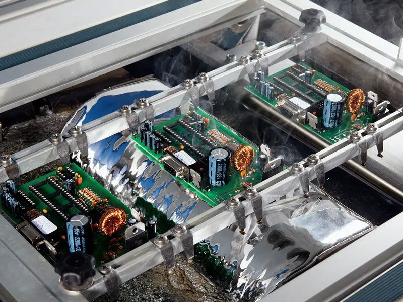
The load must reach the board in a way that does not distort it. A heatsink bolted directly to a thin board through small pads will bow the board, and the bow changes the interface gap across the device.
Where the heatsink is heavy, the board carries its mass and the vibration requirement applies to it as well as to the components. A stiffener or a chassis mounted heatsink removes that load. Our vibration notes describe the analysis.
Gap Filling and Dimensional Stack
Where the gap between the device and the heatsink is not controlled, the interface material must be chosen for the maximum gap, which penalises the nominal case.
The stack should be dimensioned from the device surface to the heatsink face, including the board thickness tolerance, the pad thickness and the solder joint. A stack that is assumed rather than calculated produces a design that works on one sample.
Electrical Isolation
Where the heatsink is grounded and the device tab is live, the interface must also be an insulator. The thermal penalty for an isolating pad is real, and it should be included in the calculation rather than discovered during test.
The isolation must be verified by a test at the working voltage, not only at the assembly stage. Our design release notes cover where the requirement is recorded.
Verification
The verification is a temperature measurement on the real assembly under the worst case load, with the heatsink and the interface in place.
Where the measured temperature exceeds the calculation, the interface is the first item to check, followed by the mounting flatness and the airflow. Our quality notes describe how the result is recorded.
Process Control and Verification
On a design of this kind, flatness is the item that decides how the rest of the board is arranged. Documenting the assumption is part of the design work, and a short note on the drawing prevents a question that would otherwise arrive a day later and cost a day of schedule. The process window is set by the narrowest step in the flow, so an improvement anywhere else shows up as margin rather than as yield until that step is addressed.
A short note on the drawing about handling, storage or packaging is often worth more than an extra decimal place on a tolerance. Where a value sits close to a process limit, the drawing should say so, since the shop can then open the process window rather than working to a nominal figure that carries no tolerance.
A stack-up that is drawn rather than described removes most of the ambiguity from a quotation, and it lets the fabricator price the board against the dielectric and copper weights that will actually be used. Where the requirement is not written down, the shop supplies its own default, and the default is chosen for the process rather than for the design.
The measurements that matter are the repeatable ones: conductor width and spacing, annular ring, finished hole size, plating thickness and surface finish are all verifiable on a coupon that travels with the panel. Running a first article through the same checks as the production panel confirms that the two agree, and that comparison is the cheapest form of process control available at prototype stage.
Process Control and Verification
On a design of this kind, flatness is the item that decides how the rest of the board is arranged. Documenting the assumption is part of the design work, and a short note on the drawing prevents a question that would otherwise arrive a day later and cost a day of schedule. The process window is set by the narrowest step in the flow, so an improvement anywhere else shows up as margin rather than as yield until that step is addressed.
A short note on the drawing about handling, storage or packaging is often worth more than an extra decimal place on a tolerance. Where a value sits close to a process limit, the drawing should say so, since the shop can then open the process window rather than working to a nominal figure that carries no tolerance.
Process Control and Verification
On a design of this kind, flatness is the item that decides how the rest of the board is arranged. Documenting the assumption is part of the design work, and a short note on the drawing prevents a question that would otherwise arrive a day later and cost a day of schedule. The process window is set by the narrowest step in the flow, so an improvement anywhere else shows up as margin rather than as yield until that step is addressed.
A short note on the drawing about handling, storage or packaging is often worth more than an extra decimal place on a tolerance.
Process Control and Verification
On a design of this kind, flatness is the item that decides how the rest of the board is arranged. Documenting the assumption is part of the design work, and a short note on the drawing prevents a question that would otherwise arrive a day later and cost a day of schedule. The process window is set by the narrowest step in the flow, so an improvement anywhere else shows up as margin rather than as yield until that step is addressed.
A first article check confirms that the process and the drawing agree on the points listed above, and that the coupon data supports the values used in the design.

Where a measurement falls outside the expected window, the sample is retained so that the cause can be established before the balance of the batch is released.
FAQ
Is a bigger heatsink always better? Only if the interface and the mounting transfer the heat to it. Beyond that point the gain is in the airflow and the interface, not in the fin area.
Can a thermal pad replace grease? It can where the gap and the pressure vary, and it costs some performance. The choice should follow the measured assembly, not the data sheet at nominal pressure.
What does gopcb provide for heatsink mounting? We provide thermal path calculation with the interface included, material selection for the gap and the pressure, dimensional stack analysis, mounting force and flatness control, isolation verification where required, and temperature measurement on the finished assembly.