Copper Pour Design Guide
A copper pour is the metal that fills the space between the traces on a layer. It is usually connected to a supply or to ground, and on most boards it covers a large fraction of the surface. The pour is often drawn automatically at the end of the layout, which is why it is also the feature that causes the most surprises: islands that carry no current, pads that cannot be soldered, and thermal reliefs that connect nothing useful.
Why a Copper Pour Is Used
The pour serves three purposes. It provides a low impedance return path for the currents that flow in the layer above or below, it spreads heat away from the components, and it reduces the amount of copper that has to be etched away.
A large area of copper also lowers the impedance of a supply net, because the resistance and the inductance of a plane are far below those of a trace. That is why a ground pour is treated as a reference rather than as a convenience.
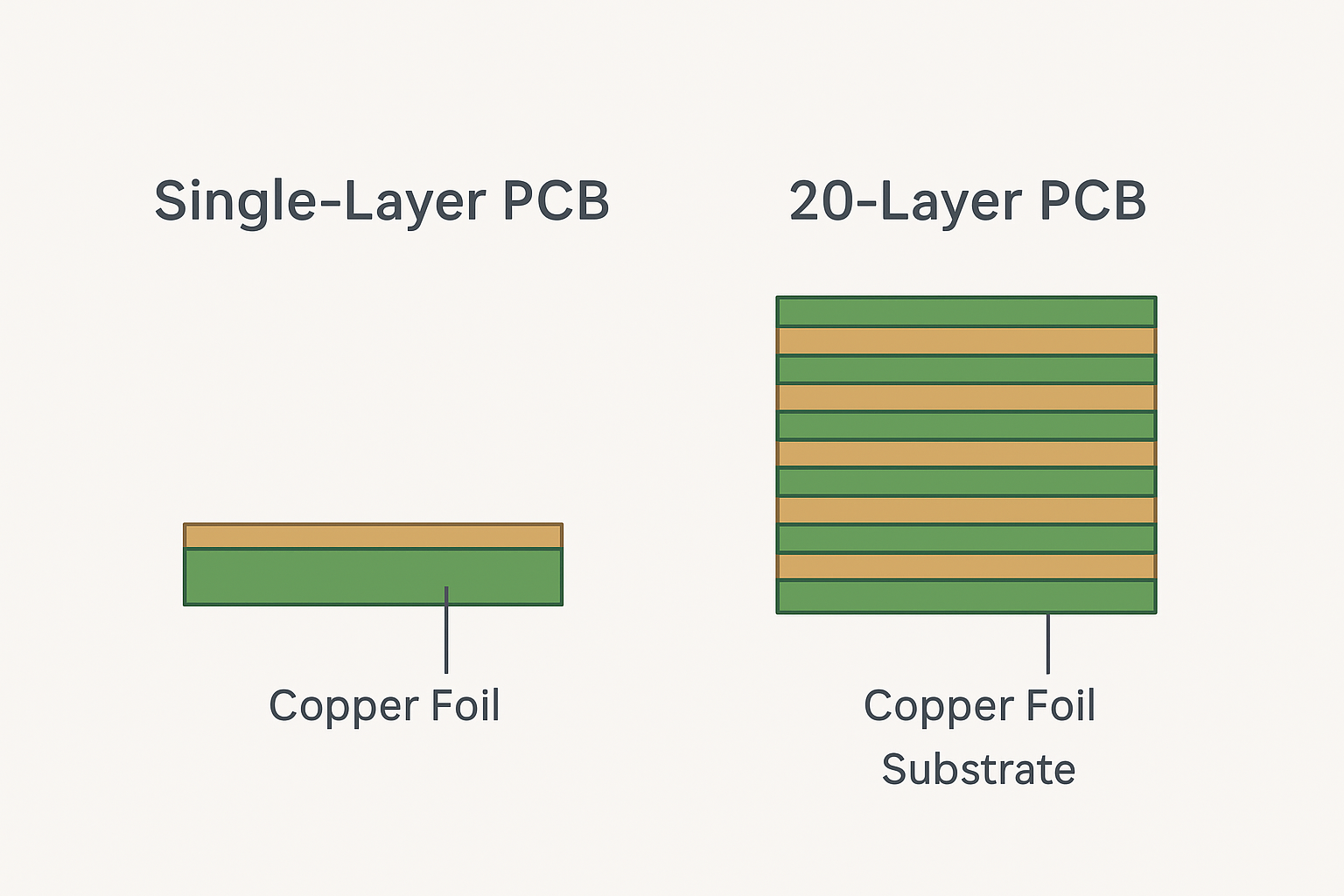
The pour also has a mechanical effect through the balance of copper across the board. An uneven distribution of copper makes the laminate distort during lamination, so a pour on a sparse layer reduces the bow and the twist.
The method of balancing copper is described in the copper balance guide, and a pour is one of the tools used for it.
Solid Pour Versus Hatched Pour
A solid pour is a continuous sheet of copper. It has the lowest impedance and the best thermal spreading, and it is the default choice on a modern board.
A hatched pour is a grid of lines with gaps between them, and it is used where the laminate and the copper have to expand at similar rates. On a large area of copper on a thin board, the difference in expansion can warp the panel, and a hatch reduces the effect.
Hatching also helps where the pour is on an outer layer of a flexible board, because a solid sheet stiffens the flex and a hatch keeps it bendable. The hatch pattern and the line width are chosen together to give a defined flexibility.
The disadvantage of a hatch is that the impedance is not well defined and the thermal spreading is poorer, so it is a compromise rather than an improvement. On a rigid board with a good balance, a solid pour is preferred.
Thermal Relief and Soldering
A thermal relief is the pattern of spokes that connects a pad to the surrounding pour. Without it the pad is attached to a plane with a very high thermal mass, and soldering it by hand or even by reflow becomes difficult.
The relief is drawn as four spokes at right angles, with a gap around the pad and the spokes crossing it. The spokes carry the electrical and thermal connection, and their width is a compromise between the soldering benefit and the impedance of the connection.
On a reflowed board the relief matters less than it does for hand soldering, because the whole panel is heated. It still matters for a pad that has to be touched up, and it matters for a pad that is connected to an inner plane by a via as well as to the pour.
The relief also affects the current path. A pin that carries a high current should have a relief with wide spokes, or no relief at all, because the spokes are a bottleneck in the connection. The current calculation applies to the spokes as much as to the trace.
Islands, Slivers and Stitching
An island is a piece of pour that is not connected to anything. It is created where traces and pads isolate an area, and it is electrically floating, which means it can act as a small antenna or as a capacitor to whatever passes nearby.
The layout tool can be set to remove islands below a certain area, and that setting should always be used. A pour with floating fragments is worse than no pour at all, because the fragments are invisible in the netlist and only appear when the impedance is measured.
A sliver is a narrow strip of pour that is isolated or barely connected. It is a fabrication problem as well, because a thin strip can lift during etching or plating, and it should be removed by the same rule that removes the islands.
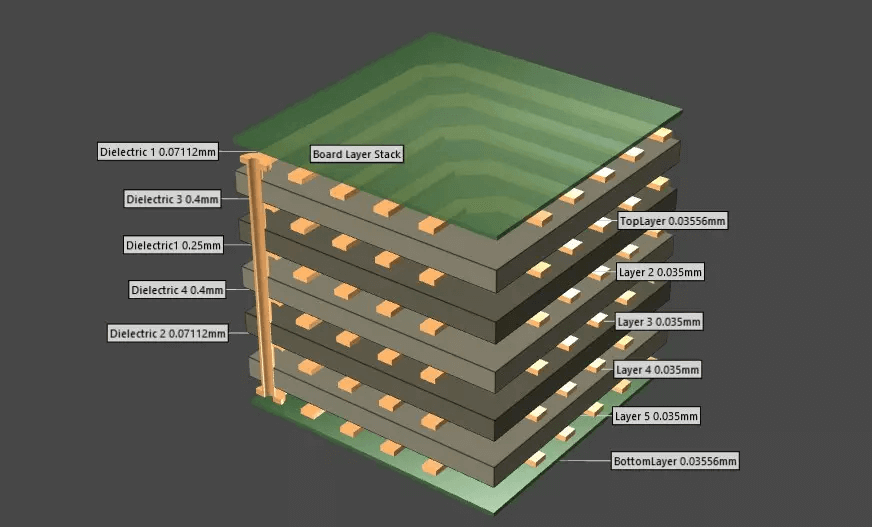
The remaining areas are tied together with stitching vias, which connect the pour on one layer to the same net on the other layers. The spacing of the stitching sets the impedance of the return path, and it should be tight enough to keep the return current close to the trace that produced it.
Current Capacity and Noise
A pour is not a substitute for a proper power plane on a high current design. The pour is interrupted by every trace that crosses it, and the current has to flow around those interruptions, which increases both the resistance and the inductance.
Where a supply has to carry a large current, the plane should be continuous on a dedicated layer, and the pour should be left to the reference net. Mixing the two on one layer creates a supply that looks solid in the drawing and is broken in the layout.
On a mixed signal board the pour is part of the reference scheme, and splitting it requires care. A split in a ground pour forces the return current to take a long path around the gap, which increases the loop area and the emissions.
The power integrity work and the crosstalk rules both depend on the plane being continuous under the traces, so the pour should be reviewed before the layout is released rather than after.
Design Review
The review starts with the net that the pour is assigned to, and with the areas where the pour must not be used. A pour that is assigned to ground by default will connect every pad that touches it, including the ones that were meant to be isolated.
The second item is the island and sliver rule, which should be set and checked rather than left at the tool default. The third is the stitching, checked against the frequency and the current path.
The fourth is the thermal relief, checked on the pads that have to be soldered and on the pads that carry current. A relief that is too narrow is a bottleneck, and one that is too wide is a soldering problem.
Finally, the pour should be regenerated after every change to the layout, because a pour is a derived feature and it does not update itself. A board that was checked before the last few traces were moved has a pour that no longer matches the design.
FAQ
Is a copper pour always a good idea? On most boards it is, because it provides a return path and spreads heat. On a board where the pour creates islands and long thin slivers, the balance can be negative and the pour should be simplified.
Why do pads have thermal relief spokes? So that the pad can be heated to soldering temperature. A pad tied directly to a large plane conducts the heat away faster than the iron or the oven can supply it.
Should stitching vias be placed on a grid? A grid is convenient, but the useful rule is to place them where the return current flows and at a spacing well under a quarter wavelength at the highest frequency of interest.