Panel Cleaning Before Lamination and Coating Steps
Between the plating line and the lamination press, and again before solder mask is applied, the panel has to be clean. Contamination at those points does not show up immediately: it appears later as a delaminated inner layer, a lifted mask or a coating that will not wet. Panel cleaning is one of the least glamorous steps in the shop and one of the most influential.
Why Panel Cleaning Matters
Lamination bonds resin to copper, and solder mask bonds polymer to copper and laminate. Both bonds depend on the surface being free of anything that forms a weak layer. An oil film, a handling residue or a friable oxide becomes the weakest link, and the failure occurs there rather than in the material.
The consequences surface much later. A delaminated inner layer may only appear after the board is heated during assembly. A mask that lifts shows up after reflow. By then the panel is finished, and the cause is several process steps away from where the defect is found.
What Has to Be Removed
Cleaning has to deal with several classes of contamination. Organic films come from fingerprints, oils from equipment and airborne deposits. Particulate contamination comes from drilling, routing and the environment. Chemical residues come from plating, etching and the cleaning process itself.
Oxide is a special case, because it is part of the copper rather than a deposit on it. A thin, dense oxide is desirable for bonding; a thick, friable one is not. Cleaning therefore has to produce a controlled surface rather than simply a physically clean one, and the distinction matters when a process is being tuned. Aggressive cleaning that strips too much oxide can leave a surface that bonds worse than a lightly oxidised one, which is a counter intuitive result until the mechanism is understood.
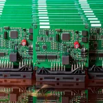
<img src="https://www.gopcba.com/wp-content/uploads/2026/08/pcb1.jpg" alt="PCB panels passing through a pumice scrubbing line before lamination” />
Mechanical Cleaning Methods
Mechanical cleaning removes deposits and lightly abrades the surface. Pumice scrubbing, brush scrubbing and abrasive wheels are all used, with the fine grade chosen to leave a controlled roughness rather than to remove copper. The aim is a consistent surface, not a deep cut.
Mechanical methods have to be controlled because they remove material. Excessive scrubbing thins the copper, particularly on fine traces, and it can round the edges of conductors in ways that affect subsequent imaging. Brush pressure, roller condition and the number of passes all belong in the process specification. The condition of the brushes or the pumice slurry is therefore a process parameter, and it should be checked on a schedule rather than when a defect appears.
Chemical Cleaning and Micro-Etch
Chemical cleaning removes organic films with an alkaline or acidic cleaner, often with surfactants and sometimes with ultrasonic agitation to reach blind features. The chemistry has to suit the soil being removed; a cleaner chosen for oils will not remove the residues left by an aggressive plating bath.
A micro-etch then removes a controlled thickness of copper along with the surface oxide, leaving a uniformly roughened surface that bonds well. The etch depth is measured in fractions of a micrometre and has to be controlled, because too little leaves oxide and too much removes the copper that the circuit needs. Related chemistry is described in this guide to PCB etching.
Oxide Treatment and Bonding
Before lamination the copper is usually treated to create a surface that the resin can bond to. Black oxide and its alternatives produce a roughened, chemically active layer that improves adhesion to the prepreg. The treatment has to be dense and well attached, because a friable layer fails within itself during thermal stress.
The treatment also has to be compatible with the resin and with the lamination cycle. A treatment that is ideal for one prepreg may bond poorly to another, and the interaction is not visible until the panels are pressed and tested. The materials involved are described in this guide to laminate material properties.
Rinsing and Drying
Rinsing is where cleaning often fails. Every cleaning chemistry leaves a residue if it is not rinsed thoroughly, and the residue becomes the weak layer that the cleaning was supposed to remove. Cascading rinses with progressively cleaner water, and a final rinse with deionised water, are the usual approach.
Drying has to remove water without leaving spots or allowing the surface to oxidise. Water quality matters because dissolved solids remain on the surface when the water evaporates, and hard water leaves visible deposits that interfere with bonding. Drying temperature and time also affect how quickly the clean surface re-oxidises.
Cleaning Before Coating and Solder Mask
Before solder mask, the surface conditions are different because the copper is already patterned and the panel has been through imaging and etching. The residues here are organic and photographic, and the cleaning step has to remove them without attacking the fine features or leaving the surface too smooth to key.
Before conformal coating the requirement is wetting rather than bonding strength. The surface has to be free of anything that raises its resistance to the coating, and the cleaning method has to be compatible with the components already fitted. The verification of surface condition before coating is discussed in this guide to judging PCB quality.
Verification Methods
Verification uses water break tests, contact angle measurement and coupon based checks. The water break test observes whether a film of water remains unbroken across the surface, which indicates a clean, high energy surface. It is quick and needs no equipment beyond a supply of clean water.
Coupon testing is more quantitative. A coupon cleaned with the production process and then bonded or coated shows whether the process produces a surface that performs. That result is more relevant than a measurement on a freshly cleaned sample that has not experienced the rest of the flow.
Process Control and Common Problems
The most common problems are a cleaner that has become loaded with contamination, a rinse that is no longer clean, a micro-etch that has drifted, and panels that are handled after cleaning. Each has a distinct signature, and each is visible if the process parameters are recorded rather than assumed.
Time between cleaning and the next step also matters. A clean surface re-contaminates and re-oxidises, so the interval should be specified and monitored, and a cleaning step that is timed rather than assumed is the practical way to keep it under control. The requirement belongs with the other process conditions in the fabrication notes, where it can be reviewed with the rest of the job.
FAQ
What is a water break test? Clean water is poured over the surface and the film is observed. If it stays unbroken for a defined period, the surface is clean enough for the next step. A film that pulls back into droplets indicates contamination or a low energy surface.
How much copper does a micro-etch remove? Typically a small fraction of a micrometre, chosen to remove the oxide and leave a uniform surface. The exact amount is process specific and is measured on a coupon, because the depth controls both the bond strength and how much copper remains on fine traces.
Why do panels delaminate if the cleaning is fine? Cleanliness is one of several inputs. Moisture in the prepreg, an oxide layer that is too thick or poorly attached, an incorrect lamination cycle and incompatible materials can all cause delamination on a panel that was cleaned correctly.