
Via Fencing and Stitching for Effective PCB Shielding
A ground plane looks like a solid reference until a signal changes layer next to it. Where a trace drops through a via, the return current has to move from one plane to another, and if there is no nearby path it takes a long detour. Via fencing and stitching are the layout practices that give the return current a short, controlled route.
What Via Fencing Does
Fencing means placing a row of ground vias alongside a signal, usually along the length of a critical trace or around the edge of a sensitive area. The vias connect the ground planes through the board, so the return current can transfer between layers close to where the signal does, and the loop area of the current path stays small.
Small loop area is the whole point. An antenna is a loop, and its efficiency depends on the area enclosed. A return path that detours around a plane split makes a large loop, and that loop both radiates the signal out and receives noise from the environment.
Return Paths and Loop Area
The return current of a microstrip or stripline trace flows in the plane directly beneath it, concentrated close to the trace at high frequency. When the trace changes layer, the return current must change planes too, and the only low impedance route is a via connected to both planes, placed near the signal via.
Without that via, the return current finds a path by capacitive coupling between planes or by going to the edge of the board and back, both of which are high impedance and create the loop. The resulting emissions appear at the frequency of the signal and its harmonics, and they are often attributed to the clock or the connector rather than to the layer transition.
Fencing Along a Trace
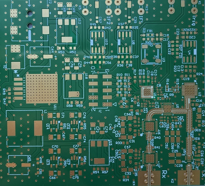
A trace that runs a long distance on an inner layer can be fenced with ground vias on both sides at regular intervals. The fence carries the return current along the trace and shields it from neighbouring nets, and the spacing between vias determines the highest frequency at which the fence behaves as a continuous wall.
Spacing is normally set to a fraction of the wavelength of the highest frequency of concern, commonly one tenth or one twentieth. Above that frequency the fence begins to leak, because the gaps between vias become electrically significant.
Stitching Between Ground Planes
Stitching is a more general version of the same idea: ground vias distributed across a board to tie all the ground planes together. The goal is a single low impedance ground system rather than several planes that are only connected at the board edge, which can behave as separate references at high frequency.
Stitching vias should follow the perimeter of the board, the edge of any plane split and the boundary of any isolated ground region. Where two grounds are joined deliberately, the joint should be a defined structure rather than an accidental one, because the impedance between two grounds is what determines how much noise crosses between them.
Spacing Rules and Wavelength
The spacing rule is a frequency rule. At one gigahertz, a wavelength in a typical dielectric is roughly one hundred and fifty millimetres, so a spacing of ten millimetres corresponds to about one fifteenth of a wavelength. Closer spacing is needed at higher frequencies or where the structure must be tighter.
The rule of thumb is that a gap smaller than one twentieth of a wavelength behaves roughly like a solid wall, while gaps larger than a quarter wavelength behave like an open slot. The transition between those two is gradual, so design to the tighter figure when the consequence of leakage is significant. The broader design context is covered in this guide to high speed PCB design rules.
Fencing Around Components and Shields
A shielding can mounted on a board needs a fence of vias around its perimeter, so that the wall of the can is continued through the board. Without it, energy escapes under the edge of the can and the shield performs worse than its material would suggest.
The same applies around connectors, crystal circuits and switching regulators, where the source of noise is localised. A ring of vias connected to the ground plane around the noisy circuit keeps the energy inside, and a corresponding ring around a sensitive circuit keeps it out.
Via Geometry and Manufacturability
Fencing and stitching vias are usually the smallest the process allows, because they carry no signal current and their only job is to provide a low inductance connection. A small via with a short barrel has low inductance, which is exactly what is wanted at high frequency.
The via must still have an adequate annular ring and must not compromise the plane it connects to. A large number of vias in a small area can also weaken the plane by removing copper and can create thermal issues during assembly, so the fence should be designed rather than poured in without thought. The fabrication constraints are described in this guide to the PCB production process flow.
Effects on Impedance and Layer Design
A ground via placed too close to a signal trace changes the local impedance, because it acts as a small capacitance to ground and because it distorts the field pattern. The effect is small when the via is at least a few trace widths away, which is another reason to space the fence rather than crowd it.
The layer stack itself determines whether fencing is possible. A design with two ground planes adjacent to the signal layers can be fenced through a short distance, while a stack where the reference layers are far apart requires long vias that are less effective. The layer arrangement is discussed in this guide to multilayer layer assignment.
Verification and Common Mistakes
The most common mistake is fencing one side of a trace and not the other, which provides a return path on one side only and leaves the other open. The second is placing the fence too far from the layer transition, so the return current still has to travel to reach it.
A third is assuming that a solid plane makes fencing unnecessary. It does not, because the plane is only a reference while the return current can stay in it; the moment the signal changes layer, the return has to change planes as well. Checking those transitions in a layout review catches more emission problems than any amount of shielding afterwards.
FAQ
How close together should ground vias be? A spacing of one tenth to one twentieth of a wavelength at the highest frequency of concern is the usual starting rule, with tighter spacing where leakage matters. Spacing also has to respect the impedance effect on any nearby signal trace.
Do I need fencing if I use a solid ground plane? Yes, at every point where a signal changes reference plane. The plane itself is continuous, but the return current has to move between planes at the transition, and only a nearby ground via provides a low impedance path for that move.
Can there be too many stitching vias? In principle yes, because each via removes copper from the plane and adds a small discontinuity. In practice the density is usually limited by drill spacing rules and by cost, and a well distributed pattern is rarely a problem.