Impedance Controlled Connector Launch Design for High Speed
A high speed link is usually designed as a clean transmission line, and then it has to pass through a connector. The launch, meaning the transition from the board traces into the connector footprint and out again, is where most of the reflection in a short channel originates. Designing that region deliberately is what separates a channel that meets its budget from one that does not.
Why the Launch Matters
The impedance of a trace is controlled by its geometry and its reference plane. At the connector, the geometry changes abruptly: the trace widens into a pad, the reference plane may be interrupted, and the return current has to find a path through the connector’s own ground structure. Every one of those changes creates a reflection.
In a long channel, the loss of the trace dominates and the launch contribution is diluted. In a short channel, such as a mezzanine or a board to board connection, the launch may be the largest single source of signal degradation, and no amount of careful trace routing will compensate for it.
The Anatomy of a Launch
A launch typically consists of the trace, a short fan out to the pad, the pad itself, a via that carries the signal through the board or to a different layer, and the ground structure of the connector. Each element has a local impedance, and the transition is only clean when those impedances match each other and the trace.
The ground path is part of the signal path. At the connector, the return current must transfer from the board ground to the connector ground, and it does so through the ground pins or the shell. If those connections are far from the signal pins, the return path is long and the launch inductance is high.

Impedance Through the Transition
The pad and the fan out are wider than the trace, so they present a lower impedance and add capacitance. The via and the vertical transition add inductance. A well designed launch arranges these so that the capacitive and inductive effects partially cancel, which is why a small amount of excess capacitance in the pad can be tolerable if the return path is kept short.
Tuning the transition means adjusting the pad size, the fan out width and the ground via placement together. Narrowing the pad reduces capacitance but makes assembly harder; adding ground vias reduces inductance but takes routing space. The balance is found by simulation and confirmed by measurement.
Ground Return at the Connector
Ground vias should be placed immediately adjacent to every signal via at the launch, ideally two per signal via on opposite sides. They provide a short return path and confine the field, which reduces both the impedance discontinuity and the radiation from the transition.
The plane under the connector also matters. A solid reference plane that extends underneath the connector footprint keeps the field controlled, while a plane that stops short forces the return current to take a longer route. Where a connector requires a cut out in the plane, the cut out should be as small as the connector allows.
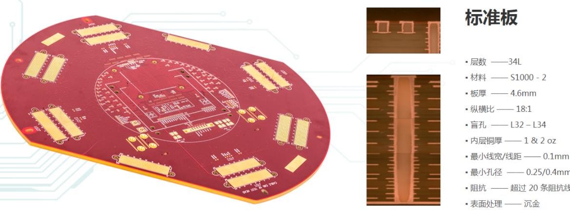
<img src="https://www.gopcba.com/wp-content/uploads/2026/05/智能电表PCBA.png" alt="Backdrilled via cross section removing a stub at a connector launch” />
Stubs and Excess Capacitance
A via that passes through the board and is not used on the layers below leaves a stub, which is an unterminated length of transmission line. At high frequency the stub resonates and produces a deep notch in the channel response, which appears as a specific frequency where the link performs badly.
Back drilling removes the unused portion of the barrel and moves the resonance far above the operating band. Where back drilling is not available, the via can be designed as a blind or buried via, or the layer stack can be arranged so that the signal transitions on a layer closer to the termination point.
Footprint and Pad Geometry
The connector footprint is usually supplied by the manufacturer with a recommended pad size. That recommendation is designed for manufacturability rather than for impedance, and for high speed applications it often needs adjustment: smaller pads, tighter fan out and a defined ground via arrangement.
Adjustments should be made with the assembly process in mind. A pad that is too small for the solder volume creates a weak joint, and a fan out that is too narrow for the current or the fabrication tolerance creates a yield problem. The compromise is normally documented as a modified footprint rather than an improvised one.
Connector Selection and Its Data
Connectors differ enormously in how well they support high speed signalling. A part specified for a data rate usually has a published insertion loss and crosstalk figure, measured in a test fixture, and those figures give an indication of how much of the channel budget the connector will consume.
The data are only comparable when the fixture and the measurement conditions are stated. A connector specified at one data rate with a particular reference launch may perform differently in a design with a different stack-up, which is why a measured evaluation on the actual board is worthwhile for critical links.
Simulation and Measurement
Simulation of the launch requires a three dimensional model, because the transition is not a simple transmission line. The model should include the via, the pad, the ground vias and the connector’s own structure, and it should be validated against a measurement on a test board.
Measurement is normally made on a coupon with the same launch, using a network analyser and a calibrated probe or a connectorised launch. The comparison between simulated and measured results is what establishes confidence in the model for the next design, and it is the point of building the test coupon in the first place.
Layout Review Checklist
A launch review should check that the signal via has adjacent ground vias, that the reference plane is continuous beneath the connector, that the fan out length is minimised, that any stub is removed or accounted for and that the pad geometry matches the assembly requirement.
The review should also confirm that the connector’s ground pins are all connected to the same ground, because a connector with several ground pins connected to different ground regions is a common source of launch problems. These checks belong with the other high speed review items, and the surrounding routing rules are described in this guide to high speed design rules.
FAQ
How much of the channel budget does a connector use? It depends on the connector and the data rate, but a well designed launch may contribute a small fraction of a decibel while a poor one with a long stub can dominate the channel. The connector data sheet gives the starting estimate.
Do I need back drilling for a connector launch? Only if the via stub is long enough to resonate within the operating band. For a thick board with a signal transitioning near the top, the stub can be significant, and back drilling or a blind via is the usual answer.
Can the launch be designed without simulation? For moderate data rates, following good practice with ground vias and short fan out is often enough. At the highest rates the transition has enough structure that a model is needed, because the interaction between the pad capacitance and the return inductance is not obvious by inspection.