Board Handling and Scratch Prevention in PCB Assembly
Most boards are damaged by the way they are moved rather than by the way they are made. A scratch across a solder mask, a chip on a panel edge, a fingerprint on a gold pad or a scuff on a finished surface are all handling defects, and they appear between the last process step that could have prevented them and the inspection that finally finds them. Good board handling is a discipline rather than a piece of equipment, and it is one of the cheapest quality measures available to any shop.
What Handling Damage Looks Like
The visible forms are scratches through the solder mask, scuffs on the surface finish, chipped panel edges, bent corners, fingerprints and local discolouration where a finger or a tool has touched a pad. Some of these are cosmetic and some are functional, and the difference is often decided by the location rather than by the size of the defect.
The damage can also be invisible. A scratch that exposes copper under a gold pad will not be seen until corrosion begins, and contamination that is not visible can prevent soldering hours later. That is why handling controls focus on preventing contact rather than on detecting its consequences.
Sources of Scratches and Scuffs
Scratches come from sliding contact. Boards stacked on a table, dragged out of a magazine, pushed across a conveyor rail or dropped into a bin all slide against something harder than the mask, and the mask is soft compared with copper, steel or ceramic. The fix is usually to stop the sliding rather than to change the material.
Equipment contributes as well. Worn conveyor rails, misaligned guides, rough edges on a fixture and burrs on a magazine slot all scrape the board as it passes, and the defect then appears at the same position on every board. A recurring scratch in one place is a strong signal that the cause is in the transport path rather than in the operator.
Gloves, Finger Cots and Skin Contact
Skin carries salts, oils and moisture, and all three are hostile to a surface finish. A fingerprint on a pad left for a few hours can oxidise and cause a soldering defect, and on a gold contact it can increase contact resistance. The control is simple: bare hands should not touch the functional areas of a board at any stage.
Gloves are not automatically the answer. Latex and nitrile gloves can carry powder from the manufacturing process, and a glove that has touched a surface or a tool can transfer contamination just as a finger would. Glove policy should specify the type, the change frequency and the areas that may be touched, with the board held by its edges whenever possible.
Conveyors, Magazines and Racks
Where boards travel, they must be supported. A conveyor that carries a board only at its edges will sag the middle of a thin panel, and the sag can crack the mask or stress a component. Edge support fingers should be clean, free of solder and set to a width that matches the panel rather than left at the last product setting.
Magazines and racks need to be sized for the board, not just for the process. A slot that is too tight grips the panel and scratches the edge; one that is too loose allows the board to move and to strike the slot wall. The rack itself should be conductive or static dissipative and checked for contamination and roughness.
Edge Chipping and Panel Breakout
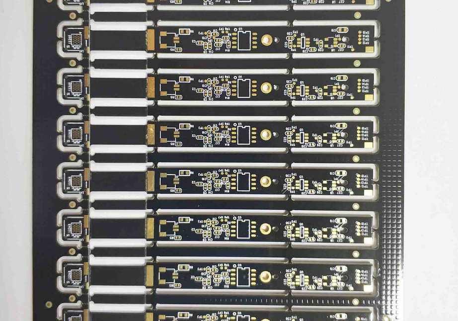
Edge damage occurs when a panel is separated and when it is handled afterwards. Routing leaves a machined edge with a defined profile, while a poor break along a score line leaves a rough edge with loose fibres and cracks that can propagate into the laminate.
Cracks that begin at the edge are a reliability concern because they can grow under thermal cycling and reach a trace or a via. Where the edge is close to functional copper, the design rules should specify the clearance and the breakout technique, and the choices available are described in the guide to breakaway tab design.
Surface Contamination and Its Effects
Contamination shows up later as a soldering defect or as a reliability problem. Oils and salts from skin inhibit wetting, silicone from a lubricant or a release agent causes voids and poor adhesion, and dust from a workshop settles on a surface and is then trapped under a component or a coating.
The effects are not limited to assembly. A contaminated surface finish corrodes faster, a contaminated gold contact wears faster, and a board that is coated over a contaminated surface may delaminate later. The material composition of the finish and its sensitivity to contamination are described in the guide to surface finishes.
Cleaning Limits and Rework
Cleaning can remove contamination but cannot repair a scratch that has exposed copper or a chip that has removed material. Where cleaning is used, it has to be appropriate to the finish and the residue, and it must not introduce its own problems such as residues from an aggressive chemistry or damage to a coated surface.
Rework of handling damage is rarely justified. Touching up a scratch with mask or paint hides the defect without restoring the surface, and the repair itself may be less reliable than the original material. The decision should be made against written criteria, and boards outside them should be scrapped rather than cosmetically improved.
Inspection and Acceptance Criteria
The criteria should define what counts as a defect and where it matters. A scratch in a non functional area may be acceptable, while the same scratch over a pad or between two traces is not. Writing the rule in terms of location and depth removes the argument that otherwise follows every borderline board.
Inspection should also record where the defect was found, because that information locates the cause. A defect rate that is tracked by process step shows whether the problem is in a machine, in a transport path or in a manual operation, and it turns a general complaint into an improvement project. The wider subject of setting and using such criteria is covered in the guide to judging PCB quality.
Training and Line Discipline
Training is what makes the rules stick. An operator who understands why a fingerprint on a gold pad matters will follow the glove policy because it makes sense, while one who has only been told not to touch the board will follow it until the shift gets busy. Short, regular refreshers work better than a single induction session.
Discipline also means making the correct behaviour easy. Racks, stands and designated holding points should be within reach of every workstation, and there should be somewhere to put a board down that is not the conveyor or the bench. Where the correct action is the easiest action, the handling standard maintains itself.
FAQ
Is a scratch through the solder mask always a defect? Not always. A scratch in an area with no copper beneath it and away from any functional feature is usually cosmetic. A scratch that exposes copper, crosses a trace or sits on a pad is a functional defect because it can corrode, bridge or interfere with soldering.
Which gloves should be used for board handling? The choice depends on the process, but the common requirements are that the glove is clean, low in particles and does not shed lint. The policy should also state how often gloves are changed and which parts of the board may be touched, and the edges of the board should be used for holding whenever possible.
Can a chipped panel edge be repaired? No. Material that has broken away cannot be restored, and filling the chip hides the crack that usually accompanies it. The edge should be evaluated against the design clearance, and a chip that reaches or approaches functional copper makes the board a scrap item.