
Copper Thickness Selection for Power and Ground Planes
A power plane is usually specified by its finished copper weight rather than by a dimension, and the two are related but not identical. The figure on the drawing sets the current the plane can carry, and it also sets what the etcher can hold.
How the Weight Is Quoted
The nominal figure refers to the foil that goes into the press. Plating adds to it, so finished copper weight on an outer layer is always higher than the starting foil, and the difference depends on the plating distribution.
The distribution is not uniform on a board with fine features and large planes. Our plating notes describe how the current is arranged.
Current Carrying Capacity
The cross section of the conductor sets the resistance, and the resistance times the current squared sets the heating. Copper thickness therefore enters the temperature rise calculation directly rather than as a margin.
Where the current is high and the area is fixed, the plane is the only practical answer. Our current capacity notes work through the arithmetic.
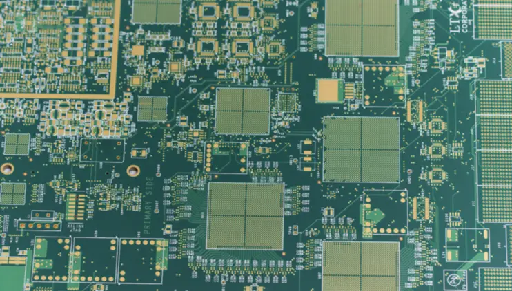
Effect on Impedance Control
On a controlled impedance layer the trace width is calculated from the dielectric height and the copper thickness. A finished thickness that is higher than the value used in the calculation gives an impedance that is lower than the target.
The calculation should therefore use the finished figure. Our high speed notes describe the tolerances that apply.
Etching Limits
Heavy copper etches differently from thin copper, because the etchant has to remove more material in the same time and it attacks sideways as well as downwards. The etching tolerance is therefore wider on a heavy layer.
The minimum space on a heavy layer should be chosen with that in mind rather than copied from a thin layer design. Our etching notes describe the compensation.
Thermal Behaviour
Copper spreads heat laterally as well as carrying current, so a thick plane changes the thermal path under a power device. That can be wanted or unwanted, and it should be a decision rather than a side effect.
Where the plane is used as a heat spreader, the thermal vias have to match it. Our thermal design notes describe the combination.
When Heavy Copper Is Worth It
Heavy copper raises the price because it needs thicker plating, longer etching and wider minimum features. It is usually worth it when the current is high enough that a thin plane would need a second layer or a bus bar.
The comparison should be made against the total solution rather than the board alone. Our metal core notes describe the alternative.
Verification
The verification is a microsection from the panel, measured for finished copper thickness on the same layer and the same feature size that the design uses. A coupon with a different pattern is not evidence.
Where the thickness is critical, the measurement should be repeated across the panel. Our test coupon notes describe the arrangement.
Process Control and Verification
On a design of this kind, etching tolerance is the item that decides how the rest of the board is arranged. A short note on the drawing about handling, storage or packaging is often worth more than an extra decimal place on a tolerance. Where a value sits close to a process limit, the drawing should say so, since the shop can then open the process window rather than working to a nominal figure that carries no tolerance.
A stack-up that is drawn rather than described removes most of the ambiguity from a quotation, and it lets the fabricator price the board against the dielectric and copper weights that will actually be used. Where the requirement is not written down, the shop supplies its own default, and the default is chosen for the process rather than for the design.
The measurements that matter are the repeatable ones: conductor width and spacing, annular ring, finished hole size, plating thickness and surface finish are all verifiable on a coupon that travels with the panel. Running a first article through the same checks as the production panel confirms that the two agree, and that comparison is the cheapest form of process control available at prototype stage.
Keeping a sample from the panel turns a dispute into a measurement, because the same coupon can be re-examined by both parties without rebuilding the batch. Reviewing the design before the data is released is cheaper than correcting it after the panel is in the tank, because every step downstream inherits the decision made at the front end.
Documenting the assumption is part of the design work, and a short note on the drawing prevents a question that would otherwise arrive a day later and cost a day of schedule.
Process Control and Verification
On a design of this kind, etching tolerance is the item that decides how the rest of the board is arranged. A short note on the drawing about handling, storage or packaging is often worth more than an extra decimal place on a tolerance. Where a value sits close to a process limit, the drawing should say so, since the shop can then open the process window rather than working to a nominal figure that carries no tolerance.
A stack-up that is drawn rather than described removes most of the ambiguity from a quotation, and it lets the fabricator price the board against the dielectric and copper weights that will actually be used. Where the requirement is not written down, the shop supplies its own default, and the default is chosen for the process rather than for the design.
The measurements that matter are the repeatable ones: conductor width and spacing, annular ring, finished hole size, plating thickness and surface finish are all verifiable on a coupon that travels with the panel.
Process Control and Verification
On a design of this kind, etching tolerance is the item that decides how the rest of the board is arranged. A short note on the drawing about handling, storage or packaging is often worth more than an extra decimal place on a tolerance. Where a value sits close to a process limit, the drawing should say so, since the shop can then open the process window rather than working to a nominal figure that carries no tolerance.
A stack-up that is drawn rather than described removes most of the ambiguity from a quotation, and it lets the fabricator price the board against the dielectric and copper weights that will actually be used.
Process Control and Verification
On a design of this kind, etching tolerance is the item that decides how the rest of the board is arranged. A short note on the drawing about handling, storage or packaging is often worth more than an extra decimal place on a tolerance. Where a value sits close to a process limit, the drawing should say so, since the shop can then open the process window rather than working to a nominal figure that carries no tolerance.
A first article check confirms that the process and the drawing agree on the points listed above, and that the coupon data supports the values used in the design.

Where a measurement falls outside the expected window, the sample is retained so that the cause can be established before the balance of the batch is released.
FAQ
Does 2 oz mean finished 2 oz? Not necessarily. The figure is usually the starting foil, and plating adds to it. The drawing should state which of the two is intended.
Can heavy copper be used on inner layers? Yes, and it is often cheaper there because the outer layers can then stay thin enough for fine pitch assembly.
What does gopcb provide for heavy copper work? We provide a stated distinction between starting foil and finished copper weight, a plating distribution plan for the board, impedance calculated from finished thickness, minimum features chosen for the heavier etch, and a microsection measured on the same feature size as the design.