PCB Etch Compensation and Finished Line Width
The copper that is imaged on the panel is not the copper that arrives at the customer. Etching undercuts the resist, plating adds thickness to the walls and the surface, and the finished line comes out narrower than the artwork. Etch compensation is the correction that brings the two together.
What the Etch Actually Removes
An etch removes copper sideways as well as downwards, and the sideways removal is what makes a fine line narrower than its artwork. The amount depends on the copper thickness, the chemistry and the time in the etcher, so a thicker copper always loses more width than a thin one.
That is why compensation is not a single number for a shop. A half ounce inner layer and a two ounce outer layer have different corrections, and applying one to the other produces a line that is either too narrow or too wide. Our etching process notes describe the chemistry side.
Imaging and the Artwork Correction
The correction is applied in the artwork rather than in the etcher, and it is expressed as an addition to the line width on the film. The addition accounts for the etch loss plus the tolerance band the finished line has to sit inside, and it is stored per layer and per copper weight.
Where the correction is wrong for the process, the line measures correctly in the middle of the panel and misses at the edges. Uniformity across the panel is the reason the correction is set from the worst case position rather than from the average. Our fabrication notes describe how that setting is recorded.
Finished Line Width and Its Tolerance
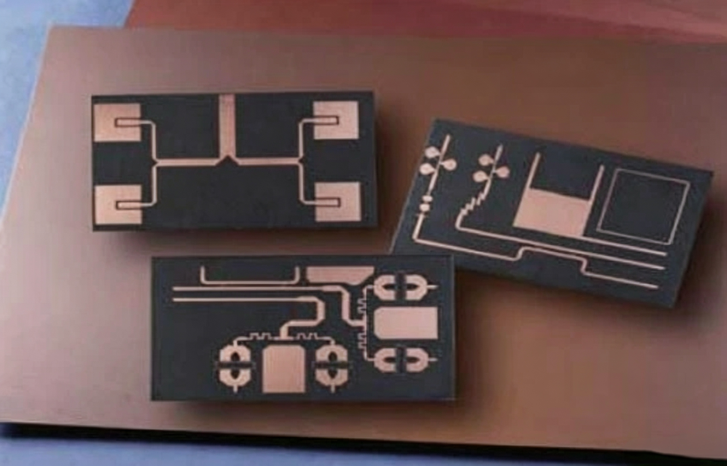
The customer specifies a finished line width with a tolerance, and the shop has to produce that after etch rather than after imaging. A tolerance that is tight enough to matter is usually quoted on the finished figure, and the correction is what makes it achievable.
Impedance controlled lines are the extreme case, because the impedance depends on the line width and on the dielectric thickness together. A width that drifts by a few microns moves the impedance by a figure that a high speed design can notice. Our plating thickness notes cover the thickness half of that pair.
Plating Before and After Etch
A pattern plated board has the copper added before the etch, so the etch sees a thick line and the correction is large. A panel plated board has the copper added afterwards, so the etch acts on the base foil and the correction is smaller but the thickness tolerance is wider.
The choice between the two is therefore a choice about which tolerance matters more. Where the line width is critical, pattern plating gives a tighter width; where the plating has to be uniform in the holes, panel plating is often easier to control.
Compensation and Annular Ring
Pads are compensated as well as lines, and the correction interacts with the drill tolerance. A pad that is compensated down for etch narrowing still has to leave an annular ring after the hole has moved, so the two allowances are taken together rather than separately.
Where the margin is thin, the ring is the item that decides the yield, and the cheapest fix is usually a larger pad rather than a tighter etch. That is a design decision that belongs on the drawing rather than in the shop.
Measuring the Result
The finished width is measured on a coupon that travels with the panel, in the same copper weight and the same position as the product. A measurement taken on the product itself is possible but destructive on most designs, so the coupon is the practical answer.
The measurement is worth recording against the etcher parameters, because a drift in chemistry or in line speed shows up as a width change before it shows up as a scrap board. Our board quality notes describe how the coupon is judged.
Thin Copper and Fine Lines
A fine line on a thin foil is easier to hold than the same line on a thick one, because the sideways etch loss scales with the thickness. That is why the highest density designs use the thinnest foil the current carrying requirement allows.
The limit is set by the current rather than by the imaging. Where the trace has to carry current, the foil cannot be thinned further, and the line width tolerance has to be negotiated against the electrical requirement instead.
Cost of Holding a Tight Width
Holding a tight finished width costs money in three places: the etching has to be run slower and more carefully, the yield falls at the edge of the tolerance and the measurement effort rises. A tolerance that is quoted without a reason for its value is often the most expensive line on the drawing.
A short note on the drawing about which traces are critical is worth more than a decimal place on all of them. Where a requirement is not written down, the shop supplies its own default, and that default is chosen for the process rather than for the design.
Process Control and Verification
On a design of this kind, imaging is the item that decides how the rest of the board is arranged. Documenting the assumption is part of the design work, and a short note on the drawing prevents a question that would otherwise arrive a day later and cost a day of schedule. The process window is set by the narrowest step in the flow, so an improvement anywhere else shows up as margin rather than as yield until that step is addressed.
A short note on the drawing about handling, storage or packaging is often worth more than an extra decimal place on a tolerance. Where a value sits close to a process limit, the drawing should say so, since the shop can then open the process window rather than working to a nominal figure that carries no tolerance.
Process Control and Verification
On a design of this kind, imaging is the item that decides how the rest of the board is arranged. Documenting the assumption is part of the design work, and a short note on the drawing prevents a question that would otherwise arrive a day later and cost a day of schedule. The process window is set by the narrowest step in the flow, so an improvement anywhere else shows up as margin rather than as yield until that step is addressed.
FAQ
Is etch compensation the same as the etch factor? No. The factor describes the sideways loss for a given thickness, and the compensation is the correction applied to the artwork using that factor plus the tolerance.
Can compensation fix a line that is too narrow in one area? It cannot. Compensation is uniform across the artwork, so a local narrowing is a process uniformity problem rather than a compensation problem.
What does gopcb provide for line width control? We provide compensation set per layer and per copper weight, coupon measurement of the finished width, plating and etch parameters recorded against the result, panel uniformity data, and records that let the same correction be reused on a repeat order.