Laser Marking: Design Rules and Process Limits
A board that can be identified can be controlled. Traceability turns a shipment into a set of individual units that can be linked to a panel, a lot, a process recipe and a test result, which is what makes containment possible when something goes wrong. Laser marking is the usual way to put that identity on the board itself, because it needs no label, survives cleaning and reflow, and can be applied at high speed. This article covers how the mark is made, where it should be placed and how its readability is verified rather than assumed.
Why Mark the Board Itself
Labels solve the problem until the product goes through a process that removes or obscures them. Reflow, wave soldering, aqueous cleaning and conformal coating all attack adhesive and print, and a label that survives assembly may still be damaged in the field. A laser mark is part of the board surface, so it goes wherever the board goes.
The second reason is space. A label needs an area clear of components and a flat surface to adhere to, and on a dense board that area does not exist. A small laser marked code can be placed in a region that no component or routing needs, and it can be read by a camera at a distance without contact.
Marking Methods Compared
Laser marking works by changing the surface, and the mechanism depends on the material. On solder mask, the laser removes or carbonises a thin layer, leaving a colour change that contrasts with the surrounding mask. On bare copper or a metal finish, the mark is produced by oxidation or by a shallow texture change rather than by material removal.
Inkjet and pad printing remain in use for cost reasons on simple products, but both add a consumable and a curing step, and both can be removed by solvents. Mechanical indentation is durable but damages the surface and is unsuitable on thin boards and on finished surfaces. For a product that needs a durable identity at a defined position, the laser is usually the best compromise.
<img src="https://www.gopcba.com/wp-content/uploads/2026/08/pcb8.jpg" alt="Laser marking head engraving a data matrix code on a printed circuit board” />
Laser Parameters and Contrast
Contrast is produced by a combination of power, pulse frequency, spot size and the number of passes, and the correct combination is different for a green mask, a black mask and an exposed metal surface. Too little energy leaves a mark that fades after cleaning or coating, and too much energy cuts through the mask and exposes the laminate underneath.
The interaction with the surface finish matters as much as the mask. A mark on bare copper oxidises and changes contrast over time, while a mark on a plated finish may reflect enough light to confuse a reader. Where the code must be read after coating, the coating itself changes the contrast, so qualification has to include the coating step rather than stop at the mark.
Data Matrix Symbols and Read Rate
A data matrix is a two dimensional symbol, which means the amount of data is limited by the number of modules rather than by the length of a printed line. The same physical area that holds a short serial number can hold a longer record, and error correction allows the code to be read even when part of it is damaged.
Read rate is the parameter to verify. Module size, quiet zone, contrast and the placement of the mark relative to board features all affect whether a camera reads it on the first attempt. A code that requires several attempts slows the line and, worse, produces intermittent traceability with gaps that are discovered only when a failure is being investigated. The verification practice used for assembly measurement data applies here: define the acceptance criterion, measure it, and record the result.
Placement and Design Rules
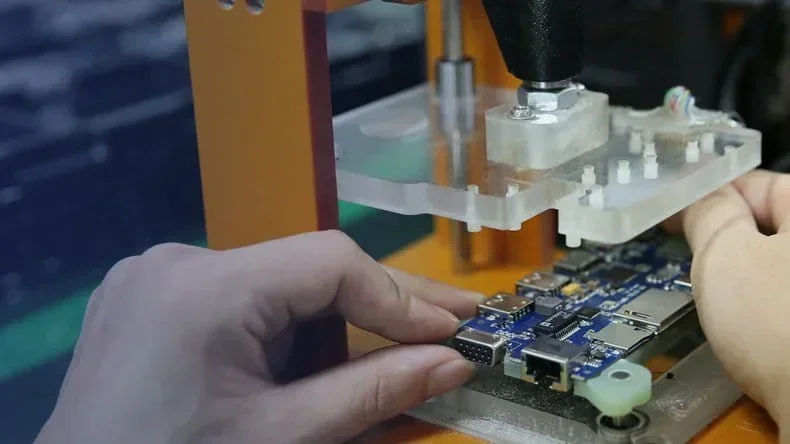
The mark needs a clear area with a defined quiet zone, and it must not be placed where it will be covered by a component, a shield or a conformal coating that is opaque. Component keep out areas and tooling holes are the usual neighbours, and the mark should be far enough from the board edge that handling equipment does not touch it.
Placement should also survive the assembly process. A mark under a connector body is invisible after assembly, and a mark on a surface that will be coated may lose contrast. The layout conventions collected in silkscreen design rules are a useful starting point for spacing, since the same clearances apply to any printed or engraved feature on the mask.
Verification and Rework Interaction
Verification should include the reading conditions used in production, not a laboratory camera in ideal light. Checking the grade of the symbol, its measured contrast and the read rate over a run of boards shows whether the process is stable, and checking after cleaning and after coating shows whether it survives the whole flow.
Marking and rework interact in a way that should be planned. A board that is reworked after marking may need a new mark or a repair record, and a mark that has been partially removed by a rework operation should not be left to look intact. Where unit level traceability is required, the record of the rework has to be attached to the same identity. The acceptance logic that governs such decisions is the same as for other production records described in PCB fabrication notes.
Panel Level and Unit Level Identity
Traceability has two levels and they should not be confused. Panel level marking identifies the manufacturing panel, which is what links a board to drilling, plating and imaging records. Unit level marking identifies the individual board, which is what links a specific assembly to its test results and its field history. Which one is required depends on the product, and the decision should be taken at design stage because it determines how much board area has to be reserved.
A common compromise is to mark the panel for fabrication and to mark the unit during assembly. That keeps the fabrication mark out of the way of components and puts the unit identity where it can be applied after the board is populated. Both marks must be readable by the same system, or the traceability chain has a break at exactly the point where data is most needed.
Durability, Cleaning and Coating
Durability testing should reflect the actual process. A mark that survives an aqueous cleaning cycle may be affected by a solvent based process, and a mark that survives both may lose contrast under a coating that fills the engraved texture. Testing the mark on a production board through the real sequence is the only convincing evidence.
Storage also matters. A mark on bare copper can continue to oxidise, and the contrast may drop slowly over months in a humid environment. Where the code must be readable after long storage, the mark should be placed on a surface whose appearance is stable, or the reading should be qualified against the aged sample rather than the fresh one.
FAQ
Can a laser mark damage the board? Yes, if the energy is too high. Cutting through the mask to the laminate is a defect, and it can also affect the electrical performance of a nearby trace.
What module size is practical? It depends on the space available and the reader, but very small modules reduce read rate and require a better camera. Choose the largest module that fits the available area.
Should the mark be readable after conformal coating? Where traceability must continue into the field, yes, and that requirement has to be confirmed on a coated sample rather than assumed from the uncoated result.