Stencil Aperture Design for Mixed Technology Boards
A mixed technology board carries a fine pitch surface mount population and a set of through hole parts, and the two need different paste volumes from the same stencil. Meeting both on one sheet of metal is the problem the stencil design has to solve.
Why One Thickness Cannot Serve Both
A fine pitch aperture needs a thin foil so that the area ratio stays high enough for the paste to release. A through hole site needs a large volume, which on a thin foil requires an aperture that is too large to print cleanly.
The two requirements are therefore separated on the board or on the stencil rather than compromised. Our paste volume notes describe the target each type of joint needs.
Step and Two Level Stencils
A stepped stencil thickens the foil at the through hole sites by etching or by welding a second sheet, so the fine pitch area keeps the thin foil. The step has a transition that has to be placed where the squeegee can cross it without leaving a trail.
A two level stencil achieves the same result by using two sheets with an overlap. Both work, and both need the squeegee and the print parameters developed for the step. Our squeegee notes describe the selection.
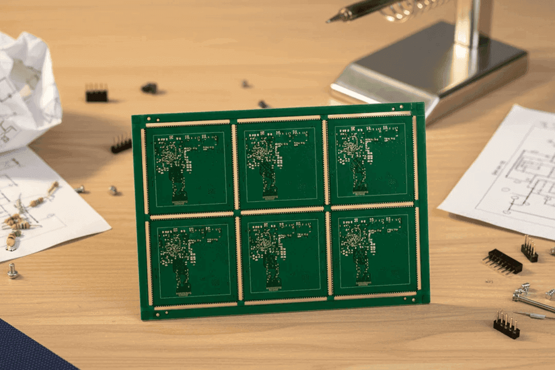
The area ratio is the aperture area divided by the wall area, and it has to stay above the value the paste can release from. A square aperture has a higher ratio than a long narrow one of the same area, so the shape matters as well as the size.
Where a pad is long and narrow, the aperture is often split into two or made slightly rounded to keep the ratio up. The change is small and it is the difference between a clean release and a partial fill. Our SPI notes describe how the result is measured.
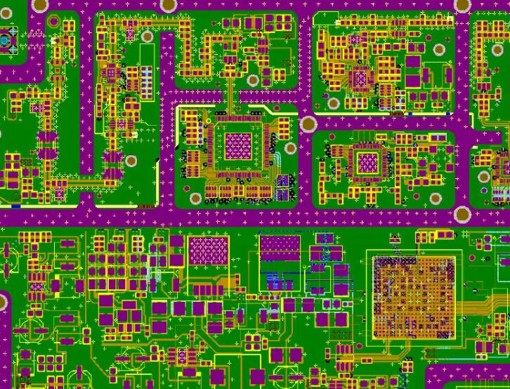
Apertures are often reduced relative to the pad to prevent bridging, and the reduction is chosen from the print result rather than from a rule. A reduction that is too large leaves a joint that is short of alloy.
The reduction is applied per aperture type rather than across the board. A general reduction that is right for the fine pitch is wrong for a large pad that needs volume.
The stencil thickness has a tolerance and the foil has to be flat. A foil that is bowed does not contact the pad evenly, and the result is a deposit that varies across the panel in a pattern that repeats with the bow.
The stencil is checked for flatness on receipt and after tensioning. A bent stencil is a print defect that looks like a paste problem. Our board quality notes describe how the print is judged.
The practical test of a stencil design is the deposit, not the drawing. A design that looks correct on paper is verified by printing the board, measuring the deposits and inspecting the release on the smallest aperture.
The check is done at the start of the run and after any change to the paste. A stencil that releases one paste cleanly does not necessarily release another.
Process Control and Verification
Where a value sits close to a process limit, the drawing should say so, since the shop can then open the process window rather than working to a nominal figure that carries no tolerance. A stack-up that is drawn rather than described removes most of the ambiguity from a quotation, and it lets the fabricator price the board against the dielectric and copper weights that will actually be used.
Where the requirement is not written down, the shop supplies its own default, and the default is chosen for the process rather than for the design. The measurements that matter are the repeatable ones: conductor width and spacing, annular ring, finished hole size, plating thickness and surface finish are all verifiable on a coupon that travels with the panel.
Running a first article through the same checks as the production panel confirms that the two agree, and that comparison is the cheapest form of process control available at prototype stage. Keeping a sample from the panel turns a dispute into a measurement, because the same coupon can be re-examined by both parties without rebuilding the batch.
Is a stepped stencil worth the cost? It is where the board has both a fine pitch area and through hole sites that need volume, which is most mixed technology boards.
Can the same stencil be used for two products? Only where the apertures coincide, which is rare, and the risk of using the wrong one is a changeover control issue.
What does gopcb provide for stencil design? We provide foil thickness and area ratio for the smallest aperture, stepped or two level construction where the volumes differ, aperture shape and per type reduction, flatness verified on receipt and after tensioning, and the design verified by measuring the deposits on the production board.
Checks Before Release
The checks that matter are the ones performed on the product rather than on a sample kept for the purpose, because a coupon that travels with the panel is the only evidence about that panel. Where a requirement can be measured, it should be measured at the point of manufacture and recorded against the board or the lot it applies to.
A parameter that is set once and never re verified drifts, and the drift is usually discovered by a defect rather than by the record. The tooling, the material and the profile form one system, and a change to any of them should be assessed against the other two before it is released.
Where the process window is narrow, the measurement resolution has to be better than the window, or the data cannot distinguish a good part from a marginal one.