
Copper Pour Versus Hatched Pour on Inner Layer Planes
Every inner layer needs some copper left behind after etching, and the question is whether that copper should be a solid plane or a grid. The choice affects impedance, thermal behaviour, laminate stress and how easily the board can be built. It is often made by habit rather than by analysis, and habits differ between design teams. This article compares solid and hatched pours on their real merits and gives a practical way to decide.
What a Copper Pour Does on an Inner Layer
A copper pour fills the unused area of a layer with metal that is normally connected to a power or ground net. It provides a low impedance return path, spreads heat away from hot components and reduces the amount of etchant that has to be consumed on a sparse layer.
Filling the area also changes the mechanical and electrical environment of everything nearby. Traces that run over a plane behave differently from traces that run over bare laminate, and the difference shows up in impedance, crosstalk and radiated emissions.
Solid Pour Advantages and Risks
A solid pour gives the lowest impedance return path and the best thermal spreading. It also makes impedance control predictable, because a trace over a continuous plane has a well defined reference at every point along its length.
The risk lies in manufacturability. Large areas of continuous copper are difficult to etch uniformly, and they can create a thermal imbalance that pulls the laminate as the stack cools after lamination. Without thieving or a balanced design, a solid pour on one layer and a sparse pattern on another is a common cause of bow and twist.
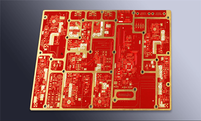
Where a solid pour is split by traces, the plane can end up in islands with narrow necks that behave like fuses under fault current rather than like a proper return path.
Hatched Pour: Lighter and More Flexible
A hatched pour replaces the solid metal with a grid, usually defined by line width and pitch. It uses less copper, which reduces the thermal mass that must be heated and cooled during lamination and therefore reduces residual stress in the finished board.
The grid also etches more uniformly, because the etchant has a shorter distance to travel and the copper density across the layer is more even. The cost is a higher impedance return path at low frequencies and a plane that behaves differently at high frequency, where the mesh may be electrically transparent or not, depending on the pitch relative to the wavelength.
Thermal Relief and Solderability
A solid plane connected directly to a through hole pulls heat away from the joint during soldering. Thermal relief spokes are the standard answer, and their geometry must be sized for the copper weight and the soldering process. On a hatched pour the same effect is milder, because the grid carries less heat away from the pad.
Neither approach removes the need for analysis. A joint that will be hand soldered needs more relief than one that goes through wave soldering, and a large via connected to a heavy plane can be difficult to fill no matter how the plane is patterned.
Warpage and Laminate Stress
Bow and twist come from unbalanced copper distribution and from differences in the thermal expansion of the materials. A hatched pour helps by making the copper density more uniform layer to layer, which is why it appears so often in thin, large boards.
The balance matters more than the pattern. Two layers with matching copper density behave well even if both use solid pours, while a solid layer paired with a nearly empty one will distort regardless of how the empty layer is filled. Check the balance before release rather than after the first panels come out of the press.
Etch Uniformity and Copper Balance
Etching large solid areas is harder than etching a grid, because the chemistry becomes depleted locally and the resist is exposed to the etchant for longer. The result can be undercut edges, uneven boundaries and a copper thickness that varies across the panel.
Copper balance is the broader principle: the amount of metal on each layer should be similar, and where it cannot be, thieving or a hatched pattern is used to fill the gap. A balanced stack etches more predictably and laminates with less movement, which is the practical reason thieving patterns exist.
High Frequency Behaviour of Hatched Planes
At high frequency the return current follows the path of least inductance, which lies directly beneath the signal trace. A solid plane supports that path everywhere. A hatched plane forces the current to weave around the grid, raising the effective inductance and, in some cases, pushing the return path to a different layer entirely.
Where the pitch of the grid is small compared with the wavelength, the hatched plane behaves much like a solid one, but the impedance is still higher and less predictable. For controlled impedance and EMC critical designs, a solid reference plane is almost always the better choice.
Deciding by Function: Ground, Power or Shield
Ask what the copper is for. A reference plane for high speed signals should be solid. A power distribution layer may tolerate hatching where the current is modest and the layer is already balanced. A shielding pour on an outer layer is usually solid around the edge of the board, where a continuous connection matters.
For mixed designs, the practical answer is often hybrid: solid under the critical interfaces and hatched elsewhere on the same layer, with the transition placed away from sensitive traces and documented on the drawing. That compromise keeps the critical nets predictable without unbalancing the whole stack.
Documenting the Choice on the Drawing
State the pour pattern, the grid pitch and width where hatched, the net the pour is connected to, and the clearance to other features. If the pour is intentionally left floating, say so, because a floating plane can behave as an antenna and is rarely what the designer intended.
gopcb reviews copper distribution as part of the fabrication review, since an unbalanced stack shows up as warpage, etch variation and assembly problems. A short note on the drawing about intent removes the guesswork and lets the shop build the layer the way it was simulated.
FAQ
Is a hatched pour always worse for signal integrity? Not always, but it raises the return path inductance and makes impedance less predictable. For controlled impedance and EMC critical nets, use a solid plane.
Does hatching reduce weight and cost? It uses less copper but adds little extra cost, since the etching and lamination steps remain. The main benefit is a more balanced stack and less laminate stress.
Can I leave a copper pour unconnected? It is possible but usually unwise. A floating plane can resonate and radiate, and it provides no return path. Connect it deliberately or remove it.