Contact Printing: Exposure Energy and Registration Accuracy
Contact printing forms the resist image by placing a photographic film directly against the resist-coated panel and exposing it through the film. The gap between film and resist is essentially zero, so the image is transferred with the resolution the film and the resist can support rather than with the resolution of a lens. It remains the standard method for the outer and inner layers of most rigid boards, and it is judged on exposure energy, film condition and registration accuracy.
What Contact Printing Is
The sequence is simple to describe. The panel is coated with photoresist, dried, and then placed in a frame with the film on one or both sides. A vacuum is drawn to bring the film into intimate contact with the resist, the lamps are switched on for a measured time, and the panel is developed so that the unexposed resist dissolves away.
Two variants are in use. In the traditional arrangement the film sits on the panel and a glass plate presses it down; in the more accurate arrangement the panel is held vertically and the film is drawn onto it by vacuum from both sides. The second gives tighter contact and is preferred where line width matters.
Exposure Energy and Photoresist Response
Photoresist responds to accumulated energy, the product of intensity and time, usually quoted in millijoules per square centimetre. Below the correct energy the resist is under-cured, so the sidewalls slope and the developed image is narrower than the film; above it the resist is over-cured, the image widens and small openings close up.
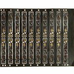
<img src="https://www.gopcba.com/wp-content/uploads/2026/06/测试-1.jpg" alt="Contact printing frame holding artwork film over a PCB panel” />
The correct energy is established with a step tablet or an exposure series for each resist type and thickness. A typical negative-working resist needs 40 to 80 mJ/cm2, and the value is confirmed by measuring the developed line width against the film dimension. Lamp ageing reduces intensity over time, so the exposure time has to be adjusted as the lamps age rather than left at the value set when they were new.
Artwork Film Condition and Handling
The film is the master, and any defect in it is reproduced on every panel. Scratches, pinholes, dust and dimensional change all matter. Film expands and contracts with temperature and humidity, which is why the dimensions of the artwork film are checked against the master and why the film is conditioned before use.
Handling matters as much as storage. Film should be held by the edges, kept in a sleeve and inspected against a light table before each use. A speck of dust on the emulsion side produces a pin hole in the resist pattern, which becomes an open circuit or a short depending on the layer.
Registration Accuracy and Tooling
Registration accuracy is the alignment between the image and the features already on the panel. It is set by the tooling system: tooling holes punched in the panel, pins in the frame, and a film that is punched to match. Every element contributes an error, and the errors accumulate along the panel.
The practical targets are tight for inner layers, where the image has to sit within the pad that the outer layer will later connect to, and looser for outer layers. Where registration is marginal, the compensating actions are a tighter tooling system, a smaller panel, or a design with more annular ring to absorb the error.
Vacuum, Contact and Feature Distortion
Good contact means no gap and no trapped air. A gap of a few tens of micrometres is enough to diffract the exposing light and to blur the image, which shows as a loss of resolution on fine lines even though the exposure energy is correct. Air trapped under the film produces the same effect locally, and it is often seen as a patch of poor definition in the middle of a large panel.
Pressure that is too high introduces a different problem. The glass plate that presses the film can deform it, and the deformation distorts the image so that lines running in one direction are displaced relative to lines running in the other. Where distortion appears only on large panels, the pressing arrangement is the first thing to examine.
Exposure Latitude and Line Width Control
Exposure latitude is the range of energy over which the developed image stays within the line width tolerance. A thick resist gives a wider latitude because more material has to be removed before the image changes, while a thin resist gives a narrower one and needs tighter control of the lamps.
The latitude also depends on the aperture size. Small openings close up quickly as energy rises, so a board with fine lines and small vias demands a tighter control than a board with coarse features. Measuring line width on a test area of every panel is the way to keep the exposure within the latitude rather than at its edge.
Comparing Contact Printing With Projection
Projection and laser direct imaging remove the film from the process, so the defects that the film carries disappear and the registration is set by the machine rather than by tooling pins. The trade is throughput and cost, and for most rigid boards with features above the fine-line range contact printing remains the economical choice.

The comparison matters for the fine-line end of the range. Where lines approach the limit of what wet etching can produce, the line width control achieved at exposure becomes a large part of the final tolerance, and a process that leaves the width slightly wider can be compensated in etching while one that is already at the limit cannot.
Common Defects and Their Causes
Pin holes come from dust or from film defects. Ragged edges come from poor contact or from a resist that was not dried properly. Line width that drifts across a panel usually indicates uneven lamp intensity or a panel that is not flat in the frame. Each of these has a different corrective action, and the pattern of the defect is what identifies it.
Where the defect repeats in the same position on every panel, the cause is in the film or in the frame rather than in the resist. Where it moves with the panel, the cause is in the resist coating or in the drying step. Keeping a reference panel and a light table image of each film makes the distinction quick.
Process Control and Records
The variables to record are the resist type and thickness, the exposure energy, the lamp condition and the last exposure series result. Line width should be measured on a defined test area after development and, later, after etching, so that the two contributions can be separated.
The section that confirms the result is taken after etching, and the standard microsection methods apply. Comparing the developed line width with the etched line width tells the shop whether a width problem belongs to the imaging step or to the etching step.
FAQ
What exposure energy should contact printing use? It depends on the resist, but 40 to 80 mJ/cm2 is a typical range for negative-working resist. The correct value is established with an exposure series and confirmed by measuring developed line width.
Why do fine lines blur even at the right energy? Usually because contact is poor. A small gap between film and resist allows the light to spread, and trapped air produces the same effect locally. Vacuum and flatness need to be checked.
Does the film change size over time? Yes. Film expands and contracts with temperature and humidity, which is why it is conditioned before use and why its dimensions are checked against the master rather than assumed.