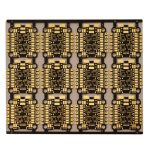
Peelable Solder Mask: Application, Cure and Peeling
A peelable solder mask is a temporary coating applied before soldering and stripped away afterwards, and it exists so that features which must remain solderable never meet the wave, the flux or the cleaning chemistry. Gold fingers on an edge connector, press-fit holes, connector cavities, mounting holes and pads reserved for a second operation are the usual candidates. The material is described by three figures rather than by a brand: applied thickness, cure condition and the peel strength at the moment of removal.
What the Coating Protects
The protection is mechanical as well as chemical. The film keeps molten solder out of a hole that has to stay open, stops flux from wicking into a connector body, and prevents the tinning of a gold finger that would otherwise lose the integrity of its plating. On a mixed assembly that is wave soldered on the secondary side, one print can protect several hundred positions at the same time.
Each use case has a different requirement. A masked hole needs a plug that survives a 250 degree Celsius wave and releases cleanly; a gold finger needs a film whose bond to the plating is weaker than the bond of the plating to the copper, or the gold lifts with the film; a connector cavity needs a coating that fills a recess without leaving voids in a corner.
Application Methods and Thickness
Screen printing is the usual method for a defined pattern, and it produces a controlled film in the range of 0.25 to 0.5 mm where wave solder protection is needed. Dispensing suits a small number of positions or a complicated outline, and spraying or dipping is used when the whole surface has to be covered and the film is removed as a single sheet.
Thickness is the first process window. Below about 0.2 mm the film can be breached by the wave crest and the protection fails silently, while a coating above about 0.8 mm traps solvent beneath its surface, cures unevenly and tends to leave fragments in a recess when it is pulled. The target thickness should be set for the feature with the greatest depth, not for the average of the pattern.
The Cure Window
Peelable materials are cured in a batch or conveyor oven at 120 to 150 degrees Celsius, and the window is narrow in both directions. An under-cured film stays tacky and weak, so it strings when it is pulled and smears into holes and along the surface it was meant to protect.
Over-cure is the more expensive failure because it is invisible until removal. The film becomes brittle, tears at the first pull instead of releasing in one piece, and can bake onto copper hard enough that the operator reaches for a scraper, which risks the plating underneath. The same principle applies to conformal coating masking, where an over-cured film cannot be pulled without damaging the surface it covered. A cure check on a coupon by thumb twist or solvent rub is more reliable than a timer, because oven loading changes the effective cure of every panel in the batch.
Peel Strength and Removal Practice
Peel strength is quoted as a force per unit width, and the figure that matters is the one measured at the temperature at which removal actually happens. A material that releases easily when warm can tear a pad when it is cold, so the removal step belongs within a defined time after soldering, while the panel is still warm, rather than the next morning.
Angle and speed matter as much as force. Pulling a tab at 45 to 90 degrees in a slow, steady motion releases the film in one piece, while a fast pull at a shallow angle concentrates stress at the edge and tears it. A tab of about 10 mm should be designed into the pattern for each protected region, positioned where an operator can reach it without touching a joint.
Residue and Cleanliness Control
The step most often skipped is verification that nothing is left behind. Silicone-based and latex-based films both leave a thin organic trace along the boundary of the former opening, and that trace either degrades solderability on the next operation or becomes a site for electrochemical migration between two conductors.
Cleanliness is measured on an extract of the board and reported as an equivalent of sodium chloride per unit area, against the 1.56 micrograms per square centimetre limit that the applicable IPC requirement sets for assemblies. A microscope check before and after cleaning catches gross film, but only the extract test finds the invisible layer left by a cleanliness measurement routine that was never applied to the masking step in the first place.
Compatibility with Wave and Reflow
A film intended for wave soldering must survive 250 to 260 degrees Celsius for three to five seconds and then the flux and the cleaning chemistry that follow. One that softens at the wave temperature can sag into an adjacent opening, and one that the flux attacks will swell and lift before anyone tries to remove it.
On a board with both a reflow and a wave step, the mask should be applied after reflow so that it never sees the full profile. Where that is impossible the material has to be qualified through both thermal cycles, and the qualification must include the peel: a film that looks intact afterwards may have cured past its usable window and will fail in the operator hands.
Inspection Before and After Removal
Before soldering the check is coverage. The film has to cover each protected feature completely, with no pinholes at a corner or along a hole edge, and an intentional overfill of about 0.5 mm around the feature is a practical way to absorb registration error. Coverage is verified visually under magnification with the board at an angle to the light.

After removal the checks are the cleanliness extract, a visual inspection of the opening at magnification, and confirmation that the protected feature is unchanged: no solder, no lifted plating and no film inside a hole. Where the hole has to accept a press-fit pin, a pin gauge is the test that settles the question, and it should be used on a sample from every panel rather than on a single board at the start of the run. Mask application records belong with the panel history so that this step is auditable like any other.
Process Window and Records
The record should carry the material lot, the applied thickness, the cure temperature and time, the interval between soldering and peeling, the peel result and the cleanliness reading. Those fields are what separate a repeatable masking step from one that works on most days and is blamed on the operator on the others.
The window is narrow because its two ends fail in opposite ways and only one of them is visible on the line: an under-cured film shows itself as a smear that the operator sees immediately, while an over-cured one leaves a fragment in a hole that is only discovered at assembly. A qualification that covers both ends, run to the applicable standard, costs far less than the rework it prevents.
FAQ
Can a peelable mask stay on the board for storage? Not as normal practice. The film continues to cure in storage, becomes brittle and may not release in one piece, so a removal time limit belongs in the process document.
Is residue a real risk? Yes. An extract cleanliness test against the applicable limit is the only reliable way to show that the film left nothing behind on a surface that has to stay solderable.
Can it protect a hole through wave soldering? It can when the plug is thick enough and cured inside its window. A film below about 0.2 mm may be breached by the wave and let solder into a hole that has to remain open.