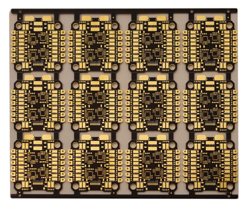
Solder Mask Over Bare Copper: SMOBC Process Control
Solder mask over bare copper describes a fabrication sequence in which the mask is printed directly onto the copper of the finished circuitry and the metallic finish is applied afterwards, only to the pads that will be soldered. The structure replaced the older practice of masking over fused tin-lead, which left plated alloy underneath the mask and was a persistent source of lifted mask, residue and unreliable adhesion. It is now the default structure for rigid boards, and the reason is process control rather than preference.
The Sequence Behind the Name
The order runs copper plating, outer layer etching, mask application, mask cure and then surface finish. Copper is plated to its finished thickness before the etch, the outer layer is patterned, and the mask is printed over the bare copper that will stay covered. Only the exposed pads receive a finish, whether that is hot air solder leveling, electroless nickel immersion gold, immersion silver, immersion tin or an organic solderability preservative.
The order matters because every finish has a thermal or a chemical cost, and in this structure the mask meets that cost after it has been cured and inspected. Applying the finish across the whole panel and masking afterwards puts the mask over a plated and fused surface, where the interface is harder to control and where residue from the finish bath is trapped under the resist.
Copper Surface Preparation Before Masking
Adhesion is decided at the interface, so the copper that will be covered has to be clean, micro-roughened and free of thick oxide. A typical preparation is a mechanical brush or pumice step followed by a chemical micro-etch that removes one to two micrometres of copper, which strips the existing oxide and leaves a thin, controlled one in its place.
The window between cleaning and mask application is short. Copper re-oxidises in air, and a surface left overnight in a humid shop carries an oxide film that reduces the peel strength of the finished mask. Where a line cannot run the two steps continuously, panels are held in a controlled atmosphere or the micro-etch is repeated immediately before printing.
Adhesion and the Cure Window
A thermal-cure liquid photoimageable mask is commonly cured at 150 degrees Celsius for 60 minutes, and the degree of cure decides both adhesion and the extent to which the finish chemistry attacks the resist. Under-cure leaves reactive groups that continue to cross-link in storage, so the mask shrinks, builds stress against the copper beneath it and can lift at a dam or a via collar.
Cure is verified rather than assumed. A differential scanning calorimetry run on a cured coupon gives the residual exotherm and therefore the degree of cure, while a solvent rub or a pencil hardness check is used routinely on the line. Adhesion is confirmed later by cross-hatch and tape tests to the applicable IPC method, repeated after thermal stress so that a marginal interface is exposed.
Finish Compatibility: Heat and Chemistry
Hot air solder leveling exposes the panel to 245 to 260 degrees Celsius for a few seconds as the alloy is blown off the pads, and the mask has to survive that shock without blistering or lifting. The shock also loads any mask that crosses a via or forms a thin dam, so the finish choice interacts with the mask geometry as well as with its cure schedule.
Electroless nickel immersion gold is chemically gentler than hot air leveling but it is not neutral. The plating bath attacks a lifted mask edge and deposits nickel under the resist, which creates a conductive path that cannot be removed by rework and shows up later as electrochemical migration. An organic solderability preservative avoids both the heat and the plating chemistry, which is why it is often paired with a fine pitch design, although it demands controlled storage and a handling limit on time to soldering.
Registration, Dam Width and Thickness
Registration is what keeps the mask off the pads, and the dam width between two adjacent pads is what keeps it in place. A minimum dam of about 0.10 mm is a common design rule on 1 oz copper, and the dam has to be narrower at the top than at the base so that the resist does not slump away from the copper it is meant to separate.

Mask thickness is measured over a trace and on a sidewall, and the two are different figures. A coating of 15 to 25 micrometres over a trace is typical for a liquid photoimageable material, with a thinner film on the vertical faces. A thickness below about 8 micrometres on a sidewall is a risk for the dielectric strength of the coating and for its performance under a thermal cycle.
The Defects This Structure Prevents
The mask covering bare copper removes the alloy layer that used to sit under the resist, and with it two failure modes that dominated earlier boards. Plated tin-lead under a mask reflows during any subsequent thermal excursion and pushes the mask away from the copper, and the residue left by the plating and fusing steps is trapped where no cleaning step can reach it.
What remains is an interface between an organic coating and a micro-etched copper surface, and that interface fails in its own ways when the preparation step is skipped. Lifting at a heat-affected area, blistering after wave soldering, and a fine network of undercut along a trace edge are all signs that the copper oxide was too thick when the mask was printed.
Inspection and Adhesion Testing
Visual inspection under low-angle light finds gross lifting, voids and contamination, and a UV or colour check confirms full coverage over the circuitry. Cross-sectioning gives the thickness over a trace and the profile of the dam, which is the measurement that a design review usually asks for on a new build.
Adhesion is quantified by a cross-hatch pattern cut through the coating and a tape pull, with the result graded against the applicable IPC acceptance table. The test is more informative when it is run after a thermal stress or a simulated reflow cycle, because that is the condition under which a weakly bonded solder mask adhesion actually loses its grip on the panel.
Process Window and Records
The window is described by the micro-etch depth, the surface roughness, the mask viscosity and print parameters, the pre-cure and final cure temperatures, and the finish conditions. Copper oxidation between the etch and the print is the variable that is hardest to see and easiest to lose, so the hold time between the two steps belongs in the record as a measured figure rather than as a note.
The record should also carry the peel test result after thermal stress, the measured mask thickness over a trace and on a sidewall, and the finish bath parameters for the run, together with the flux residue result from the final clean. With those fields a lifted mask can be traced either to the copper preparation or to the cure, and the difference matters because the two have completely different corrective actions on the shop floor.
FAQ
What does SMOBC stand for? Solder mask over bare copper. The mask is applied to bare copper circuitry and the solderable finish is applied afterwards to the exposed pads only.
Why is masking over bare copper preferred? Because it removes the alloy layer under the resist, which was a source of lifted mask and trapped residue, and it gives a more controllable interface between the coating and a micro-etched copper surface.
Which finish suits this structure best? There is no single answer. Hot air leveling tests the thermal stability of the mask, electroless nickel immersion gold tests its chemical resistance, and an organic solderability preservative is the mildest for the coating but imposes tighter storage control.