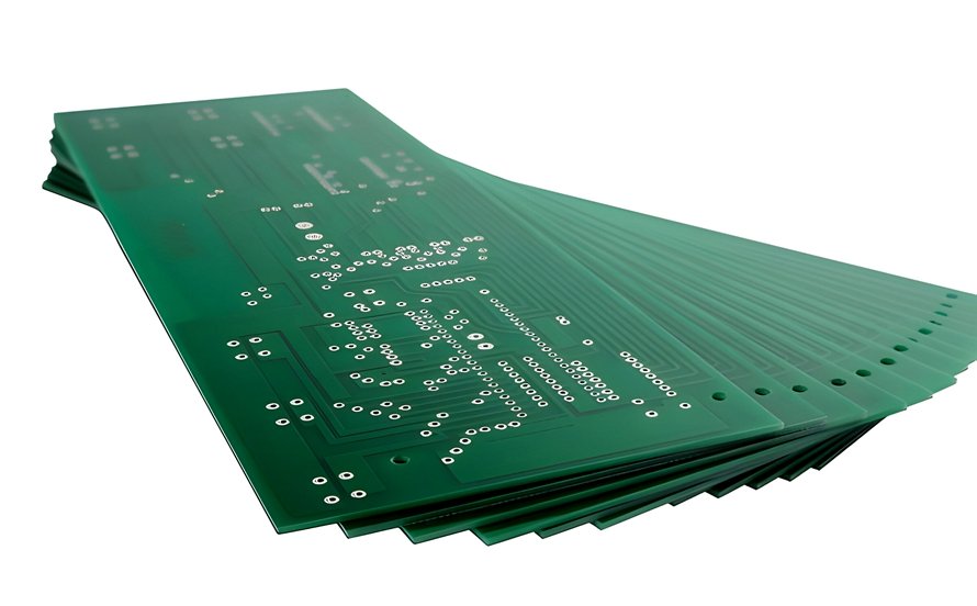
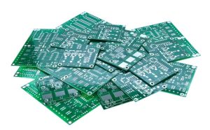
A Custom PCB is a printed circuit board specifically designed and manufactured to meet the electrical, mechanical, thermal, and functional requirements of a particular electronic product. Unlike standard off-the-shelf circuit boards, a custom PCB can be tailored to the application’s exact requirements, including board dimensions, layer count, substrate material, copper thickness, board thickness, surface finish, impedance, component layout, and other manufacturing parameters.
Custom circuit boards are widely used when a standard PCB cannot provide the required performance, form factor, functionality, or integration level. By optimizing the PCB around the complete product design, engineers can achieve better space utilization, electrical performance, thermal management, reliability, and manufacturing efficiency.
From consumer electronics and industrial equipment to automotive, medical, aerospace, and communication systems, Custom PCB Design plays an important role in developing compact and high-performance electronic products.
What Is a Custom PCB?
A Custom PCB is a circuit board engineered according to the specific requirements of an electronic application rather than a standardized board format.
During the design and manufacturing process, engineers can customize parameters such as:
- Board length, width, and shape
- Number of PCB layers
- Copper thickness
- Board thickness
- Base material
- Dielectric thickness
- Surface finish
- Minimum trace width and spacing
- Controlled impedance
- Via structures
- Solder mask color
- Component placement
- Thermal management structure
- Mechanical mounting features
This flexibility allows the PCB to be integrated more effectively into the final product.
For example, a compact wearable device may require a small multilayer PCB with a customized outline, while a high-power industrial controller may require thick copper, enhanced thermal management, and a more robust substrate.
Advantages of Custom PCB Design
Greater Design Flexibility
One of the most important advantages of Custom PCB Design is the ability to optimize the board around the specific requirements of the application.
Engineers can define the circuit layout, component locations, routing strategy, layer stackup, and mechanical dimensions according to the complete product architecture.
This flexibility is particularly valuable when a design includes:
- Specialized sensors
- High-speed interfaces
- High-density components
- RF circuits
- Power electronics
- Complex control systems
- Unique mechanical structures
Instead of adapting the product to a standard PCB, the PCB itself can be designed around the product.
Optimized Size and Space Utilization
Space is often one of the most important constraints in modern electronics.
A Custom Circuit Board can be designed to fit precisely inside the product enclosure. Engineers can optimize component placement, routing, layer count, and board geometry to make better use of the available space.
Multilayer PCB structures can further increase routing density while keeping the board footprint relatively small.
This is particularly important for:
- Smartphones
- Wearable devices
- Cameras
- IoT products
- Portable medical devices
- Compact industrial controllers
- Automotive electronic modules
For products with irregular mechanical structures, custom board outlines can also help maximize the available internal space.
Better Electrical Performance
Custom PCB development allows electrical characteristics to be considered during the earliest stages of design.
Engineers can optimize:
- Signal routing
- Ground planes
- Power distribution
- Return paths
- Controlled impedance
- Differential pairs
- High-speed interfaces
- Crosstalk reduction
- EMI and EMC performance
For high-speed products, appropriate stackup design and controlled impedance routing can help maintain signal integrity and reduce transmission-line problems.
Thermal Management
Electronic components continue to become smaller while their power density increases.
A custom board can incorporate thermal-management strategies such as:
- Large copper areas
- Thermal vias
- Copper planes
- Optimized component placement
- Metal-core construction
- Heat-spreading structures
- Dedicated thermal paths
This is especially useful for power supplies, motor controllers, LED systems, automotive electronics, and industrial equipment.
Potential Long-Term Cost Savings
Although the initial engineering cost of a custom board may be higher than using a standard PCB, customization can reduce overall product costs when the design is optimized correctly.
A well-designed custom PCB can:
- Reduce unnecessary components
- Minimize material waste
- Improve assembly efficiency
- Reduce board size
- Reduce wiring and connectors
- Lower rework requirements
- Improve product reliability
- Simplify future production
Therefore, cost should be evaluated across the entire product lifecycle rather than based solely on the unit price of the PCB.
Applications of Custom PCB
The use of Custom PCB technology has expanded across almost every major electronics industry.
Consumer Electronics
Smartphones, tablets, laptops, cameras, gaming devices, and wearable products all require highly optimized circuit-board structures.
For example, smartphones combine processors, memory, cameras, sensors, wireless communication, power-management circuits, and high-speed interfaces within a very limited space.
A custom PCB allows engineers to integrate these functions while maintaining the required electrical and mechanical performance.
Typical applications include:
- Smartphones
- Tablets
- Laptops
- Digital cameras
- Smart watches
- Fitness devices
- Portable electronics
- IoT products
Industrial Electronics
Industrial equipment often requires reliable operation under demanding environmental conditions.
Custom boards can be designed according to the equipment’s specific requirements for temperature, vibration, power consumption, communication, and control.
Applications include:
- Industrial controllers
- Automation equipment
- Motor-control systems
- Power supplies
- Sensors
- Measurement instruments
- Factory automation systems
- Communication equipment
A customized design also allows engineers to integrate control, sensing, communication, and power functions into a more compact system.
Automotive Electronics
Modern vehicles contain a large number of electronic control systems.
Custom PCB Manufacturing is widely used for applications such as:
- Engine control systems
- Battery management systems
- ADAS electronics
- Automotive lighting
- Infotainment systems
- Instrument clusters
- Motor-control modules
- Charging systems
- Power electronics
Automotive PCBs may need to withstand temperature cycling, vibration, humidity, and electrical transients. Therefore, material selection, reliability design, and manufacturing process control are particularly important.
Medical Devices
Medical electronics require high levels of reliability, accuracy, and functional stability.
Custom circuit boards can be designed for specific medical applications, including:
- Diagnostic equipment
- Patient monitoring systems
- Portable medical devices
- Laboratory instruments
- Imaging equipment
- Therapeutic equipment
Depending on the application, the PCB may need to meet strict requirements for signal integrity, electrical isolation, reliability, cleanliness, and traceability.
Aerospace and Defense Electronics
Aerospace electronics operate under demanding environmental and reliability conditions.
Custom PCBs may be used in:
- Avionics
- Navigation systems
- Communication equipment
- Control systems
- Sensors
- Monitoring systems
- Power-management equipment
Designers must consider temperature variation, vibration, weight, electromagnetic compatibility, reliability, and long-term operating stability.
Custom PCB Manufacturing Process
A successful Custom PCB Manufacturing project requires close coordination between design engineering and PCB manufacturing.
1. Requirement Collection
The first step is to define the technical and mechanical requirements of the project.
Important specifications may include:
- Electrical schematic
- PCB dimensions
- Layer count
- Material type
- Board thickness
- Copper thickness
- Minimum trace width and spacing
- Hole sizes
- Impedance requirements
- Surface finish
- Operating temperature
- Current and voltage requirements
- Component package types
- Production quantity
Environmental conditions such as temperature, humidity, vibration, and chemical exposure should also be considered where applicable.
A clear specification at the beginning of the project helps prevent costly redesigns later.
2. PCB Design and Layout
After the requirements are confirmed, engineers develop the PCB layout.
The layout process normally includes:
- Component placement
- Routing
- Power distribution
- Ground-plane design
- Via arrangement
- Thermal design
- Signal-integrity analysis
- Mechanical verification
For high-speed designs, engineers should pay particular attention to return-current paths, differential-pair routing, impedance control, crosstalk, and electromagnetic interference.
3. DFM Review
Before production, the design should undergo a Design for Manufacturability (DFM) review.
DFM evaluates whether the design can be manufactured consistently using the selected production process.
Typical checks include:
- Minimum trace width
- Minimum spacing
- Hole diameter
- Aspect ratio
- Copper distribution
- Annular ring
- Board edge clearance
- Solder mask design
- Component clearance
- Panelization
- Manufacturing tolerances
Early DFM analysis can reduce production risks and avoid unnecessary engineering changes.
4. PCB Prototype
A PCB Prototype is an important stage in custom PCB development.
Prototype boards allow engineers to verify:
- Electrical functionality
- Component compatibility
- Mechanical fit
- Signal performance
- Thermal behavior
- Assembly process
- Firmware or system integration
Depending on the product, prototypes may undergo functional testing, electrical testing, environmental testing, thermal testing, vibration testing, or other qualification procedures.
Prototype validation helps identify problems before mass production.
5. PCB Manufacturing
After the design has been validated, the PCB enters production.
A typical manufacturing process may include:
- Material preparation
- Inner-layer imaging
- Etching
- Lamination
- CNC drilling or laser drilling
- Copper plating
- Outer-layer imaging
- Etching
- Solder mask application
- Surface finishing
- Electrical testing
- Routing or V-scoring
- Final inspection
The exact process depends on the PCB structure, material, layer count, and manufacturing requirements.
6. PCB Assembly
After PCB fabrication, components can be installed through PCB Assembly processes.
Two common assembly technologies are:
- Surface Mount Technology (SMT)
- Through-Hole Technology (THT)
Some products use both technologies in the same assembly.
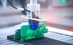
The assembly process may include solder paste printing, component placement, reflow soldering, through-hole soldering, inspection, and functional testing.
Automated optical inspection (AOI) and X-ray inspection can also be used when appropriate.
Challenges in Custom PCB Development
Although customization provides significant flexibility, it also introduces additional engineering challenges.
Design Complexity
High-density and high-speed circuit designs can create problems involving signal integrity, power integrity, electromagnetic interference, thermal management, and manufacturability.
For example, poor routing can increase crosstalk or create unfavorable return-current paths.
Engineers can address these problems through techniques such as:
- Controlled impedance
- Differential-pair routing
- Proper grounding
- Power and ground planes
- Signal isolation
- Appropriate layer stackup
- Thermal optimization
Modern PCB design software and simulation tools can also help identify potential problems before fabrication.
Manufacturing Limitations
Every PCB manufacturer has process capabilities and tolerances that must be considered during design.
Common limitations include:
- Minimum trace width
- Minimum spacing
- Minimum hole diameter
- Maximum aspect ratio
- Copper thickness
- Registration accuracy
- Board thickness tolerance
- Surface-finish requirements
A design that exceeds the selected manufacturer’s process capability may increase cost or reduce production yield.
For this reason, engineers should communicate with the PCB manufacturer early rather than waiting until the final production stage.
Cost Management
Cost is another important consideration in custom PCB development.
The total cost may be influenced by:
- Board size
- Layer count
- Material selection
- Copper thickness
- Via technology
- Surface finish
- Production volume
- Component density
- PCB assembly requirements
- Testing requirements
For example, increasing the number of layers may improve routing density but also increase material and manufacturing costs.
Engineers should therefore balance performance, reliability, manufacturability, and cost instead of optimizing only one factor.
How to Choose a Custom PCB Manufacturer
Selecting the right manufacturing partner is critical for a successful custom PCB project.
Important factors include:
Engineering Capability
The manufacturer should be able to understand PCB design requirements and provide practical DFM feedback.
Engineering support is particularly important for complex multilayer, high-speed, high-current, HDI, rigid-flex, and other specialized PCB designs.
Manufacturing Capability
The manufacturer’s capabilities should match the actual requirements of the project.
Important considerations include:
- Supported layer counts
- Material options
- Copper thickness
- Board thickness
- Minimum trace and spacing
- Via technology
- Surface finishes
- PCB assembly capabilities
- Testing capabilities
Quality Control
Quality control should be implemented throughout the manufacturing process rather than only during final inspection.
Depending on the project, quality-control procedures may include:
- Automated optical inspection
- X-ray inspection
- Electrical testing
- Dimensional inspection
- Solderability testing
- Cross-section analysis
- Final visual inspection
The appropriate inspection plan should be determined according to the PCB’s application and reliability requirements.
Why Choose Kingda for Custom PCB Manufacturing?
Kingda provides customized PCB manufacturing solutions for customers with different electrical, mechanical, thermal, and production requirements.
Instead of applying a single standard PCB configuration to every project, Kingda can work with customers to evaluate the appropriate board structure according to the product’s actual requirements.
The customization process can cover:
- PCB material selection
- Layer configuration
- Board thickness
- Copper thickness
- Surface finish
- Controlled impedance
- Via structures
- Board dimensions
- Thermal-management requirements
- Prototype production
- PCB assembly
- Manufacturing optimization
For complex projects, early engineering communication can help identify potential design and manufacturing risks before production.
Engineering-Focused PCB Solutions
A successful Custom PCB Manufacturing project is not simply about producing a circuit board according to a set of files. It also requires coordination between PCB design, material selection, manufacturing processes, assembly, testing, and final application requirements.
Kingda focuses on providing practical PCB manufacturing support throughout the product development process, helping customers balance performance, reliability, manufacturability, and cost.
Whether the project involves a compact consumer device, industrial controller, automotive module, medical instrument, or other specialized electronic product, selecting an appropriate Custom PCB structure can provide greater flexibility for optimizing the final system.
Conclusion
A Custom PCB provides engineers with the flexibility to develop a circuit board around the specific requirements of an electronic product.
Compared with standard PCB solutions, customized boards can offer better control over size, electrical performance, thermal management, component integration, and mechanical compatibility.
However, successful customization requires more than simply changing the board dimensions. Material selection, stackup, impedance, thermal design, DFM, prototyping, manufacturing, assembly, and testing should all be considered as part of an integrated development process.
By working with an experienced manufacturing partner such as Kingda from the early design stage, customers can better align PCB design with manufacturing capabilities and develop reliable, cost-effective circuit boards for their specific applications.