How to Design a PCB: PCB Design, PCB Manufacturing & Step-by-Step Guide
Printed circuit boards (PCBs) are the foundation of modern electronics. From consumer devices and industrial equipment to automotive systems, medical instruments, and communication products, PCBs provide the physical and electrical platform that connects electronic components and enables a complete system to function.
The quality of a finished electronic product is strongly influenced by the quality of its PCB Design. A well-engineered board can improve electrical performance, reliability, manufacturability, thermal management, and product longevity. In contrast, design mistakes can lead to signal integrity problems, overheating, assembly defects, costly redesigns, and production delays.
For beginners, learning how to design a PCB may initially seem complicated. However, when the process is divided into clearly defined stages, PCB design becomes much easier to understand and manage.
This step-by-step guide explains how to design a PCB, from defining requirements and creating the schematic to layout, verification, manufacturing files, and prototyping.
What Is PCB Design?
PCB Design is the engineering process of converting an electronic circuit concept and schematic into a physical printed circuit board that can be manufactured and assembled.
The process combines electrical engineering, mechanical design, component selection, signal integrity, thermal management, manufacturability, and design verification. Whether the project involves a simple single-sided PCB or a sophisticated multilayer board, the designer must translate the circuit’s electrical relationships into a practical physical layout.
A typical PCB design workflow includes:
- Defining electrical and mechanical requirements
- Creating the circuit schematic
- Selecting appropriate components
- Creating the physical PCB layout
- Defining layer stackup
- Routing traces and critical signals
- Designing power and ground distribution
- Running ERC and DRC checks
- Reviewing DFM and assembly requirements
- Generating Gerber and other manufacturing files
- Building and testing a prototype
Understanding these fundamentals is essential for anyone learning how to design a reliable and manufacturable PCB.
How Is a PCB Designed?
A professional PCB design process consists of several interconnected stages. Although individual projects may require additional steps, the following workflow provides a practical foundation for beginners.
1. Define the Purpose and Requirements
Before opening PCB design software, clearly define what the board needs to accomplish.
Start by creating a detailed requirements list covering both electrical and mechanical requirements. Depending on the project, this may include:
- Operating voltage and current
- Power consumption
- Board dimensions
- Board shape and mounting locations
- Number of PCB layers
- Component types and package sizes
- Operating temperature
- Environmental conditions
- Communication interfaces
- High-speed or high-frequency requirements
- Regulatory and safety requirements
- Expected production volume
- Cost and manufacturing constraints
The requirements should also identify special design considerations such as controlled impedance, isolation distances, thermal requirements, connector locations, and enclosure limitations.
A clear specification at the beginning of the project reduces redesigns later. It also gives the PCB designer and manufacturer a common reference for evaluating the design.
2. Create the Circuit Schematic
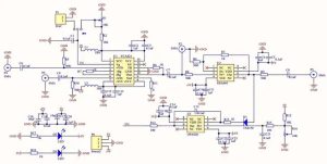
The schematic is the electrical blueprint of the PCB. It defines how components are electrically connected before those connections are converted into a physical board layout.
Professional PCB design software such as Altium Designer, KiCad, or other EDA platforms can be used to create and manage schematics.
At this stage, designers should:
- Place all required components in the schematic
- Define electrical connections between components
- Assign appropriate component values
- Select suitable footprints
- Identify power and ground connections
- Add net labels and circuit annotations
- Define design constraints where necessary
- Run an Electrical Rules Check (ERC)
The schematic should be organized according to circuit function. For example, power management, analog circuits, digital logic, RF sections, processors, memory, and communication interfaces can be grouped into logical blocks.
Good schematic organization makes the later PCB layout process easier and helps engineers identify design errors before physical routing begins.
It is also important to verify component ratings. Voltage rating, current rating, power dissipation, tolerance, package dimensions, operating temperature, and availability should all be considered during component selection.
3. Design the PCB Layout
Once the schematic has been verified, the electrical design is transferred into the physical PCB layout.
This is one of the most important stages of the entire PCB Design process. The designer must determine where each component will be located and how electrical connections will be routed between them.
The layout should balance electrical performance, thermal behavior, mechanical requirements, assembly efficiency, and manufacturability.
Determine the Board Configuration
First determine the basic board structure.
Important considerations include:
- Board length and width
- Board thickness
- Number of copper layers
- Copper weight
- Dielectric material
- Controlled-impedance requirements
- Surface finish
- Solder mask requirements
- Mounting holes
- Connector locations
For standard applications, FR-4 is widely used. High-frequency or specialized applications may require materials such as PTFE-based laminates or other high-performance dielectric systems.
The required layer count depends on routing density, power distribution, signal integrity, thermal requirements, and mechanical limitations.
Place Components Strategically
Component placement has a major influence on PCB performance and manufacturability.
Components should generally be grouped according to their function. For example:
- Power components should remain close to their associated circuits.
- Decoupling capacitors should be placed close to IC power pins.
- High-speed interfaces should have short and direct signal paths.
- Analog and sensitive circuits should be protected from noisy switching areas.
- RF components should follow the required RF signal path and keepout rules.
- Heat-generating components should have sufficient copper area and thermal paths.
Connectors should also be positioned according to the mechanical enclosure and system requirements.
Good component placement can significantly reduce unnecessary routing, parasitic effects, electromagnetic interference (EMI), and assembly complexity.
Route Traces and Critical Signals
After component placement, the designer routes electrical connections between components.
Trace width and spacing should be selected according to the electrical and manufacturing requirements of the project.
For power traces, the designer must consider current capacity and temperature rise. For high-speed signals, trace geometry, reference planes, impedance, return paths, and routing topology become particularly important.
Good routing practices include:
- Keep critical signal paths short where appropriate.
- Maintain appropriate trace-to-trace clearance.
- Avoid unnecessary sharp direction changes.
- Minimize routing discontinuities.
- Maintain continuous reference planes for high-speed signals.
- Separate sensitive signals from noisy switching nodes.
- Route differential pairs according to their impedance and length requirements.
- Consider return-current paths instead of focusing only on the forward signal path.
Critical signals should generally receive priority during routing. High-speed, clock, differential, RF, and other sensitive nets may need to be routed before less critical connections.
Design Ground and Power Planes
A properly designed ground system is essential for stable PCB operation.
In multilayer boards, dedicated ground and power planes can provide low-impedance current paths and help improve signal integrity and EMI performance.
However, simply adding a ground plane does not automatically solve every noise problem. The designer must consider current return paths, plane splits, component placement, via transitions, and the relationship between signal layers and reference planes.
For high-speed designs, maintaining a continuous reference plane beneath critical traces can help control impedance and provide a predictable return-current path.
Define the PCB Stackup
The PCB stackup describes how copper and dielectric layers are arranged within the board.
A multilayer stackup may contain:
- Signal layers
- Ground planes
- Power planes
- Prepreg dielectric layers
- Core dielectric layers
Stackup selection directly affects routing capability, controlled impedance, power distribution, thermal behavior, mechanical characteristics, and electromagnetic compatibility.
For high-speed PCB Design, stackup planning should be performed early rather than treated as an afterthought. Designers may need to work with the PCB manufacturer to confirm available materials, dielectric thicknesses, copper weights, and impedance capabilities.
4. Perform Design Verification
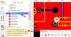
After completing the layout, the design must undergo systematic verification before manufacturing.
Design verification helps identify problems that may not be obvious from visual inspection.
Common verification methods include:
- Design Rules Check (DRC)
- Electrical Rules Check (ERC)
- Signal integrity analysis
- Power integrity analysis
- Thermal analysis
- Mechanical clearance verification
- 3D enclosure and component clearance checks
- DFM review
- DFT review
Check PCB Design Rules
The DRC should verify requirements such as:
- Minimum trace width
- Minimum trace spacing
- Via dimensions
- Hole diameter
- Annular ring
- Copper-to-edge clearance
- Solder mask clearance
- Component-to-component spacing
- Unconnected nets
- Manufacturing constraints
Clearance is particularly important because insufficient spacing can increase the risk of electrical shorts and assembly problems.
Verify Mechanical Compatibility
The PCB must physically fit into the final product.
Check:
- Board outline
- Mounting holes
- Connector positions
- Component height
- Keepout areas
- Enclosure interference
- Heat sink locations
- Cable and harness access
A PCB that passes electrical checks but cannot fit into its enclosure is still a failed design.
Review Thermal Performance
Heat-generating components should be evaluated during the design stage.
Thermal considerations may include:
- Copper area
- Thermal vias
- Heatsinks
- Component spacing
- Airflow
- Power dissipation
- PCB material
- Enclosure thermal conditions
Thermal analysis becomes particularly important for power electronics, automotive systems, LED drivers, industrial equipment, and other high-power applications.
Review Silkscreen and Assembly Information
The silkscreen should clearly identify component references, polarity indicators, connectors, test points, and other important assembly information.
Reference designators should not overlap component pads or critical soldering areas. Markings should also correspond correctly with the actual component orientation and footprint.
5. Prepare Manufacturing Files
Once the design has passed verification, manufacturing documentation can be generated.
This stage connects PCB Design with PCB Manufacturing.
The Gerber file format is commonly used to communicate PCB layer information to the manufacturer. Depending on the manufacturing process and supplier requirements, the production package may include:
- Gerber files
- Drill files
- Board outline files
- Fabrication drawings
- Stackup information
- Material specifications
- Copper weight requirements
- Surface finish requirements
- Solder mask information
- Silkscreen information
- Assembly drawings
- Pick-and-place files
- Bill of Materials (BOM)
- Special manufacturing instructions
Modern workflows may also use ODB++ or IPC-2581, depending on the manufacturer’s preferred data format.
Before releasing the files, perform a final manufacturing data review. Confirm that the correct revision is being used and that all files correspond to the same design version.
Work With the PCB Manufacturer
Communication between the designer and manufacturer is essential.
A professional manufacturer can review the design for manufacturability and identify potential production risks before fabrication begins.
This is where Design for Manufacturing (DFM) becomes particularly valuable.
DFM review may identify:
- Trace and spacing limitations
- Drill-size problems
- Insufficient copper clearance
- Difficult-to-manufacture features
- Excessively small components or pads
- Stackup limitations
- Fabrication tolerance issues
- Solder mask and silkscreen conflicts
Working with a capable PCB manufacturing partner early in the process can reduce engineering changes, manufacturing delays, and unexpected costs.
For integrated PCB fabrication and assembly services, Kingda can support the transition from design review and DFM to PCB fabrication and assembly.
6. Build and Test a PCB Prototype
Creating a prototype is the final major step before moving into larger-scale production.
A prototype allows engineers to verify whether the physical board actually performs as expected.
Prototype testing may include:
- Power-up testing
- Functional testing
- Electrical measurements
- Signal integrity testing
- Communication interface testing
- Thermal testing
- Mechanical fit testing
- EMI/EMC evaluation where applicable
- Connector and cable verification
- Firmware and hardware integration testing
If problems are discovered, the design can be revised before mass production.
For example, prototype testing may reveal:
- Incorrect component values
- Unexpected voltage levels
- Excessive temperature rise
- Signal integrity problems
- EMI issues
- Mechanical interference
- Incorrect component orientation
- Insufficient clearance
- Manufacturing or assembly defects
The objective is not simply to make the prototype work once. The goal is to validate that the design can reliably transition into repeatable PCB Manufacturing and PCB assembly.
Common PCB Design Mistakes Beginners Should Avoid
Beginners often focus on making the circuit electrically functional while overlooking manufacturing and system-level requirements.
Common mistakes include:
1. Starting Layout Before Understanding the Requirements
A designer should not begin placing components without knowing board dimensions, connectors, mounting requirements, electrical constraints, and manufacturing limitations.
2. Ignoring Component Availability
A theoretically ideal component may be unavailable, obsolete, or difficult to source. Component lifecycle and supply-chain considerations should therefore be included during design.
3. Poor Decoupling Capacitor Placement
Decoupling capacitors that are electrically connected but physically far from IC power pins may not provide the intended high-frequency performance.
4. Poor Ground Return Paths
High-speed signals need predictable return-current paths. Unnecessary plane splits or discontinuities can increase loop area and contribute to signal integrity and EMI problems.
5. Ignoring Thermal Management
High-power components require appropriate copper area, thermal vias, heat spreading, and sometimes additional cooling solutions.
6. Skipping DFM Review
A design that looks perfect in CAD software may still be difficult or expensive to manufacture.
7. Treating DRC as the Entire Verification Process
A board can pass DRC and still contain functional, thermal, mechanical, or signal-integrity problems. DRC is an important automated check, but it does not replace engineering review and prototype testing.
PCB Design vs. PCB Manufacturing
It is important for beginners to understand the difference between PCB Design and PCB Manufacturing.
PCB Design focuses on creating the electrical and physical definition of the board. It includes schematic capture, component selection, placement, routing, stackup planning, verification, and manufacturing-data preparation.
PCB Manufacturing focuses on physically producing the bare PCB from the design data. It includes processes such as imaging, etching, lamination, drilling, copper plating, solder mask application, surface finishing, electrical testing, and final inspection.
After bare-board fabrication, PCB assembly adds electronic components through processes such as SMT, THT, soldering, inspection, and functional testing.
Understanding this distinction helps designers create boards that are not only electrically correct but also practical to fabricate and assemble.
How to Improve PCB Design Quality
A reliable PCB design process should consider the entire product lifecycle rather than treating PCB layout as an isolated CAD task.
A practical approach is to:
- Define requirements before schematic capture.
- Select components based on electrical, mechanical, thermal, and supply-chain requirements.
- Organize the schematic clearly.
- Plan the layer stackup early.
- Place critical components before routing.
- Prioritize high-speed, power, RF, and other critical nets.
- Design predictable power and ground return paths.
- Apply appropriate DRC and electrical constraints.
- Perform DFM and DFT reviews.
- Check mechanical and thermal requirements.
- Generate and review complete manufacturing documentation.
- Build a prototype and test it systematically.
- Correct root causes rather than simply treating individual symptoms.
- Validate the revised design before mass production.
This methodology reduces the risk of costly redesigns and improves the transition from engineering development to production.
How Kingda Supports the PCB Development Process
For companies that need to move from circuit concepts to production-ready boards, selecting an experienced manufacturing partner can simplify the overall development process.
Kingda provides integrated PCB and PCBA capabilities, supporting projects from engineering and DFM review through PCB fabrication, component assembly, inspection, and testing.
For engineering teams, this type of integrated workflow can improve communication between PCB designers, manufacturing engineers, procurement teams, and assembly specialists.
Early collaboration is especially useful for complex boards involving multilayer structures, HDI, high-speed signals, high-frequency circuits, rigid-flex construction, heavy copper, or other specialized requirements.
Conclusion
Learning how to design a PCB is not simply about drawing traces between components. A successful board requires a systematic engineering process that connects electrical requirements, mechanical constraints, thermal management, signal integrity, manufacturability, and testing.
The process begins with clearly defining the product requirements, followed by schematic development, component selection, PCB layout, stackup planning, routing, design verification, manufacturing documentation, and prototype testing.
For beginners, the most important lesson is to think beyond the CAD screen. A good PCB Design should not only function electrically; it should also be reliable, manufacturable, serviceable, and suitable for repeatable production.
By combining careful engineering practices with DRC, DFM, DFT, prototype testing, and close communication with a qualified manufacturing partner, designers can significantly reduce production risks and create reliable products that transition more smoothly into PCB Manufacturing.
Article Summary
This guide explains how to design a PCB step by step, covering requirements definition, schematic capture, component placement, PCB layout, routing, grounding, stackup design, DRC/DFM verification, Gerber and manufacturing-file preparation, and prototype testing. By following a structured PCB Design workflow and considering PCB Manufacturing requirements from the beginning, beginners and experienced engineers alike can create more reliable, cost-effective, and manufacturable circuit boards.