ELIC PCB: Every Layer Interconnect, HDI PCB Design & PCB Manufacturing Guide
As modern electronics continue to become smaller, faster, and more multifunctional, engineers face increasing challenges when designing high-density circuit boards. A compact electronic device may contain hundreds of components, including fine-pitch BGAs, processors, memory devices, sensors, RF circuits, and high-speed interfaces. Placing, routing, and electrically isolating these components within a limited PCB area requires advanced interconnection technology.
Traditional multilayer PCB structures can become restrictive when routing density increases. Conventional through-hole vias consume valuable routing space because they extend through multiple PCB layers, while conventional blind and buried vias may still limit routing flexibility.
ELIC PCB technology provides another approach.
ELIC, or Every Layer Interconnect, is an advanced HDI PCB technology that enables interconnection between different PCB layers using copper-filled microvias. Instead of restricting each via to a predefined layer transition, an ELIC structure can provide greater routing flexibility across the entire multilayer stackup.
This technology is particularly valuable for compact electronics that require high wiring density, fine-pitch components, high-speed signal transmission, and efficient use of PCB space.
This guide explains what ELIC PCB is, how Every Layer Interconnect works, common HDI stackup structures, ELIC PCB manufacturing processes, advantages and challenges, applications, and the key factors engineers should consider when designing an ELIC board.
What Is ELIC PCB?
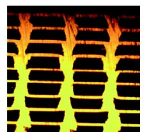
ELIC stands for Every Layer Interconnect. It is an advanced HDI PCB construction in which copper-filled microvias provide interconnections between successive layers of the PCB stackup.
ELIC is also commonly associated with Any-Layer HDI, because the technology allows circuit designers to establish connections between different layers without being restricted to conventional through-hole via structures.
The fundamental difference between a conventional multilayer PCB and an ELIC PCB is the way vertical interconnections are created.
A conventional PCB may rely heavily on through-hole vias. A traditional HDI PCB may combine through vias, blind vias, buried vias, and microvias. In an ELIC structure, copper-filled microvias are used extensively to create highly flexible layer-to-layer connections.
A simplified ELIC structure can be represented as:
Copper Layer → Microvia → Copper Layer → Microvia → Copper Layer
Each microvia is formed within a dielectric build-up layer and then metallized and filled with copper.
This construction allows routing to transition between layers while occupying a relatively small footprint.
Why Is ELIC Important for HDI PCB Design?
Modern electronic devices increasingly require:
- Smaller PCB dimensions
- Higher component density
- Fine-pitch BGA packages
- Shorter electrical interconnections
- Higher routing density
- Better signal-integrity control
- More compact layer structures
- High-speed digital interfaces
- RF and wireless functionality
Traditional vias can become a major limitation in these designs.
Because ELIC uses small microvias rather than relying exclusively on large through-holes, designers can route signals more efficiently around fine-pitch components.
This makes ELIC PCB Design particularly valuable for smartphones, wearable devices, advanced computing systems, automotive electronics, medical equipment, and other compact electronic products.
ELIC PCB Layer Stackup
The stackup is one of the most important elements of an ELIC PCB.
Unlike a conventional multilayer PCB, an ELIC structure uses sequential HDI build-up technology to create interconnections across the board.
A typical structure may include:
- Copper foil
- Dielectric material
- Copper-filled microvias
- Core material
- Additional dielectric layers
- Additional copper layers
Microvias can be arranged as stacked or staggered structures depending on the electrical and manufacturing requirements.
The final number of layers depends on the application. ELIC PCBs can be designed with structures such as 4-layer, 6-layer, 8-layer, 10-layer, 12-layer, or more complex configurations.
However, there is no universal maximum layer count for ELIC technology. The practical limit depends on the PCB manufacturer’s equipment, materials, lamination capability, registration accuracy, copper plating, microvia technology, and design requirements.
Therefore, designers should avoid specifying an arbitrary maximum layer count and instead work with the manufacturer to establish a manufacturable stackup.
Common HDI Stackup Structures
Although ELIC provides highly flexible interconnection capabilities, designers still need to select an appropriate HDI stackup.
Two commonly discussed HDI structures are 1+N+1 and 2+N+2.
1. 1+N+1 HDI Stackup
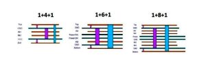
A 1+N+1 construction uses one sequential HDI build-up layer on each side of an N-layer core.
In simplified form:
HDI Build-Up + N-Layer Core + HDI Build-Up
The structure provides an additional routing layer on each side and is often used for compact products requiring moderate routing density.
Typical applications may include:
- Mobile electronics
- Portable devices
- Fine-pitch BGA products
- Compact consumer electronics
The exact number of copper layers depends on how the core and build-up layers are defined by the manufacturer.
2. 2+N+2 HDI Stackup
A 2+N+2 construction uses two sequential HDI build-up layers on each side of the core.
In simplified form:
2 HDI Build-Up Layers + N-Layer Core + 2 HDI Build-Up Layers
This provides greater routing capacity than a 1+N+1 construction.
A 2+N+2 structure can be useful for:
- Higher pin-count BGA devices
- Advanced processors
- High-density computing systems
- Communication equipment
- Complex multilayer PCB designs
The additional build-up layers increase routing flexibility but also introduce additional manufacturing complexity.
ELIC PCB Microvia Technology
Microvias are fundamental to ELIC technology.
A microvia is a very small blind-via structure, commonly produced using laser drilling. IPC technical materials commonly associate microvias with blind structures having a diameter of approximately 150 μm (6 mil) or less.
The actual minimum diameter used in production depends on:
- Laser equipment
- Dielectric thickness
- Copper thickness
- Material system
- Aspect ratio
- Pad diameter
- Registration tolerance
- PCB manufacturer’s process capability
After laser drilling, the hole is cleaned and metallized before being filled or plated as required by the ELIC structure.
Copper-Filled Microvias
Copper filling is particularly important in advanced ELIC structures.
A copper-filled microvia can provide a solid conductive path between adjacent layers and can support stacking of multiple microvias.
Copper-filled structures are also useful for via-in-pad applications because they can be planarized to provide a relatively flat surface for component placement.
Stacked vs. Staggered Microvias in ELIC PCB
ELIC PCB designs may use either stacked or staggered microvias.
Stacked Microvias
Stacked microvias are vertically aligned.
For example:
Layer 1 → Microvia → Layer 2 → Microvia → Layer 3
The microvias share approximately the same vertical footprint.
Advantages
- Excellent space utilization
- Very high routing density
- Suitable for fine-pitch BGA packages
- Efficient vertical interconnection
- Supports highly compact PCB layouts
Challenges
- Higher manufacturing complexity
- Tight registration requirements
- Copper filling may be required
- Higher process-control requirements
- Potentially higher manufacturing cost
Staggered Microvias
Staggered microvias are offset horizontally.
For example:
Layer 1 → Microvia → Layer 2
followed by an offset microvia:
Layer 2 → Microvia → Layer 3
The lateral offset can reduce some of the process challenges associated with vertically stacked microvias.
Advantages
- Greater manufacturing flexibility
- Reduced dependence on perfect vertical alignment
- Useful for high-density routing
- Can simplify certain HDI structures
Challenges
- Requires additional PCB area
- Routing may become more complicated
- Less space-efficient than directly stacked microvias
The appropriate structure should be determined according to the component pitch, routing density, reliability requirements, and manufacturing capability.
ELIC PCB vs. Conventional PCB
The primary difference between ELIC and conventional PCB technology is the interconnection architecture.
| Feature | ELIC PCB | Conventional Multilayer PCB |
|---|---|---|
| Primary interconnection | Copper-filled microvias | Often through vias, with optional blind/buried vias |
| Routing density | Very high | Moderate to high |
| Fine-pitch BGA support | Excellent | Depends on via and escape-routing strategy |
| Layer-to-layer flexibility | Very high | More restricted |
| PCB miniaturization | Strong capability | More limited |
| Manufacturing complexity | High | Generally lower |
| Manufacturing cost | Generally higher process complexity | Generally lower for comparable simple structures |
| Via-in-pad integration | Highly suitable | Possible but may require additional processing |
| Design complexity | High | Low to moderate |
| Typical applications | Compact, high-density electronics | Broad range of electronic products |
The table should not be interpreted as meaning that ELIC is always superior or less expensive. ELIC is an advanced manufacturing technology intended to solve specific density and interconnection challenges.
ELIC PCB Advantages
1. Higher Routing Density
The most important advantage of ELIC is its ability to increase routing density.
Copper-filled microvias occupy significantly less PCB area than conventional through-hole structures, allowing designers to route more signals through a compact area.
This is especially valuable underneath and around fine-pitch BGA packages.
2. Smaller PCB Form Factor
ELIC can help engineers achieve smaller circuit boards without necessarily increasing the number of conventional through-hole connections.
This makes the technology suitable for miniature electronic products.
3. Improved Layer Utilization
Because interconnections can be created between successive layers, each layer can be used more efficiently for routing.
The result is greater flexibility during PCB layout.
4. Support for Fine-Pitch Components
Modern processors, memory devices, and BGA packages often contain hundreds or thousands of connections.
ELIC microvias can provide an efficient escape-routing solution for these high-density packages.
5. Shorter Signal Paths
Microvias generally create shorter vertical transitions than long through-hole structures.
For high-speed circuits, reducing unnecessary via length can help control parasitic effects and signal-integrity challenges.
However, actual signal performance depends on the complete PCB stackup, dielectric properties, trace geometry, reference planes, via structure, and routing strategy.
6. Better Use of PCB Space
ELIC allows engineers to make greater use of available space between components and across individual routing layers.
This is especially important when board dimensions are strictly limited.
7. Support for High-Speed Applications
High-speed interfaces require carefully controlled impedance, return paths, and interconnections.
The compact via structures available in ELIC designs can support high-speed routing when properly integrated with the overall stackup and signal-integrity strategy.
8. Potential Reduction in PCB Layer Count
In some designs, ELIC can achieve a required routing density with fewer layers than would otherwise be necessary.
However, this is design-dependent. ELIC does not automatically reduce layer count or manufacturing cost.
ELIC PCB Challenges
Despite its advantages, ELIC introduces significant manufacturing and design challenges.
1. Higher Manufacturing Complexity
ELIC requires advanced HDI manufacturing processes, including laser drilling, microvia metallization, copper filling, sequential lamination, and highly accurate layer registration.
Each additional process step introduces another manufacturing variable that must be controlled.
2. Higher Process Requirements
Microvia dimensions are extremely small.
Therefore, manufacturers need accurate control over:
- Laser drilling
- Hole cleaning
- Desmear
- Copper deposition
- Copper filling
- Lamination
- Registration
- Imaging
- Etching
- Surface finishing
3. Higher Initial Cost
The specialized equipment and additional processing required for ELIC can increase manufacturing costs compared with simpler multilayer PCB structures.
However, the overall system cost should be evaluated together with board size, layer count, component density, assembly requirements, and product performance.
4. More Difficult PCB Rework
The higher density of an ELIC PCB can make troubleshooting, repair, and rework more challenging.
Internal microvias cannot be inspected in the same way as exposed conventional vias.
Therefore, reliable electrical testing and manufacturing inspection are particularly important.
5. Tight Registration Requirements
The alignment between successive HDI layers must be carefully controlled.
Any significant registration error can affect:
- Microvia landing
- Pad connection
- Annular ring
- Trace clearance
- BGA escape routing
- Electrical reliability
6. Material Selection
Material selection is particularly important for high-speed ELIC applications.
Engineers should consider:
- Dielectric constant
- Dissipation factor
- Thermal expansion
- Glass-transition temperature
- Z-axis expansion
- Copper adhesion
- Lamination characteristics
- High-frequency electrical behavior
The appropriate material depends on the application rather than simply choosing a material with the lowest dielectric constant.
ELIC PCB Manufacturing Process
The manufacturing process for ELIC PCB is more sophisticated than conventional PCB fabrication.
A typical process may include the following stages.
Step 1: Inner-Layer Circuit Fabrication
The inner copper layers are imaged, developed, etched, and inspected according to the PCB design.
AOI may be used to detect potential circuit defects.
Step 2: Sequential Lamination
Dielectric materials and copper foils are sequentially laminated to create the HDI build-up structure.
Temperature, pressure, heating rate, and lamination time must be carefully controlled.
Step 3: Laser Drilling
Laser drilling creates microvias within the HDI dielectric layers.
The laser parameters must be matched to the material system and required hole geometry.
Step 4: Hole Cleaning and Desmear
After drilling, residues may remain inside the microvias.
Cleaning and desmear processes prepare the hole walls for reliable copper metallization.
Step 5: Copper Metallization
The microvias are metallized to establish electrical conductivity.
For advanced ELIC structures, the microvias may subsequently be filled with copper.
Step 6: Copper Filling
Copper filling creates a solid conductive structure within the microvia.
This is particularly important when microvias are stacked or incorporated into via-in-pad designs.
Step 7: Additional Build-Up
Additional dielectric and copper layers are added through sequential lamination and HDI processing.
The process continues until the required stackup is completed.
Step 8: Circuit Imaging and Etching
Each build-up layer is patterned according to the PCB design.
Trace width, spacing, pad geometry, and registration must remain within the specified manufacturing tolerances.
Step 9: Surface Finishing
The finished PCB receives an appropriate surface finish, such as:
- ENIG
- ENEPIG
- OSP
- Immersion tin
- Immersion silver
- HASL, where appropriate
The correct finish depends on assembly requirements, component type, storage conditions, reliability requirements, and product application.
Step 10: Electrical and Quality Testing
ELIC PCBs should undergo appropriate inspection and testing, which may include:
- AOI
- Electrical testing
- Microsection analysis
- X-ray inspection
- Dimensional inspection
- Surface-finish inspection
- Reliability testing
The exact inspection plan depends on the product’s quality requirements and applicable standards.
IPC Standards Related to ELIC and HDI PCB
Engineers should use relevant IPC standards when designing and manufacturing ELIC PCBs.
IPC-2226
IPC-2226 provides generic design information for high-density interconnect structures and microvia technologies.
It is an important reference when establishing HDI design requirements.
IPC-6016
IPC-6016 addresses qualification and performance specifications for HDI layers and boards.
It is particularly relevant to manufacturers establishing HDI production and qualification requirements.
IPC/JPCA-2315
IPC/JPCA-2315 provides information related to HDI and microvia design rules and structure selection.
These standards should be used together with the PCB manufacturer’s manufacturing capabilities and the requirements of the final application.
Designers should always verify the current revision of applicable IPC standards before releasing production data.
ELIC PCB Applications
The ability to achieve high routing density makes ELIC suitable for many advanced electronic products.
1. Smartphones and Portable Electronics
Smartphones require extremely compact PCBs while integrating processors, memory, cameras, wireless communication, sensors, power-management circuits, and high-speed interfaces.
ELIC technology can provide the interconnection density required within a restricted board area.
2. Wearable Devices
Smartwatches, smart bands, and other wearable products require:
- Small dimensions
- Low weight
- High component density
- Low power consumption
- Wireless connectivity
- Sensor integration
ELIC PCB technology can support these compact designs.
3. Automotive Electronics
Modern vehicles contain increasingly sophisticated electronic systems, including:
- Infotainment
- Wireless charging
- Advanced driver-assistance systems
- Camera systems
- Lighting control
- Seat electronics
- Sensor modules
- Communication modules
ELIC can be considered when these functions require highly compact, high-density electronic assemblies.
4. Communication Equipment
Telecommunication and networking systems often involve high-speed signals and dense component placement.
ELIC can support compact interconnection structures when combined with appropriate high-speed PCB materials and controlled-impedance design.
5. Industrial Electronics
Industrial IoT devices, controllers, measurement systems, and automation equipment can benefit from high-density PCB technology when space and functionality requirements are demanding.
6. Medical Electronics
Medical equipment often combines sensors, processors, communication circuits, and power-management functions within compact assemblies.
ELIC can provide an interconnection solution for applications where PCB size and routing density are important.
7. Computing and High-Speed Electronics
High-performance processors, memory devices, and advanced computing modules can generate extremely high routing requirements.
ELIC provides designers with additional options for managing dense BGA escape routing and multilayer interconnections.
How to Design a Reliable ELIC PCB
A successful ELIC PCB Design requires cooperation between the PCB designer, component engineer, signal-integrity engineer, and PCB manufacturer.
The following factors should be considered early in development:
Component Pitch
Identify the smallest component pitch before selecting the via structure.
Fine-pitch BGA packages may require microvias or via-in-pad structures.
Stackup
Develop the stackup before completing high-speed routing.
Signal layers should have appropriate reference planes and controlled dielectric structures.
Microvia Geometry
Define:
- Microvia diameter
- Pad diameter
- Aspect ratio
- Capture-pad size
- Copper thickness
- Registration tolerance
based on the manufacturer’s actual capabilities.
Signal Integrity
Analyze:
- Controlled impedance
- Differential-pair routing
- Return-current paths
- Via transitions
- Crosstalk
- Power integrity
- Reference-plane continuity
Thermal Reliability
The thermal expansion behavior of the dielectric and copper structures should be considered carefully.
Repeated thermal cycling can place mechanical stress on microvia structures.
DFM Review
A comprehensive DFM review should be completed before releasing production files.
Important DFM checks include:
- Minimum trace width
- Minimum spacing
- Microvia diameter
- Pad size
- Via-to-copper clearance
- Via stacking
- Copper filling
- Layer registration
- Lamination structure
- Surface finish
- Material availability
ELIC PCB vs. Rigid-Flex PCB
ELIC and rigid-flex PCB technologies solve different engineering problems.
ELIC primarily addresses high-density interconnection and routing, while rigid-flex technology combines rigid and flexible sections to provide mechanical flexibility.
In some products, these technologies may be used independently or integrated into a broader electronic packaging strategy.
Therefore, ELIC should not be considered simply a replacement for rigid-flex PCB. The appropriate technology depends on whether the primary requirement is routing density, mechanical flexibility, packaging geometry, or a combination of these factors.
How to Choose an ELIC PCB Manufacturer
Selecting an experienced manufacturer is particularly important for ELIC projects because the manufacturing tolerances are significantly tighter than those required for many conventional PCB designs.
Before starting production, ask the manufacturer about:
- HDI manufacturing capability
- Laser drilling capability
- Copper-filled microvia technology
- Stacked and staggered microvia capability
- Sequential lamination
- Via-in-pad processing
- Layer-registration accuracy
- Minimum trace and spacing
- Available PCB materials
- AOI and electrical testing
- Microsection analysis
- Relevant IPC qualifications and certifications
- Prototype and mass-production capability
- DFM engineering support
A capable supplier should be able to review the stackup, Gerber/ODB++ data, drill files, material selection, and manufacturing tolerances before production begins.
For complex ELIC projects, early DFM collaboration can prevent expensive redesigns and manufacturing problems.
Conclusion
ELIC PCB, or Every Layer Interconnect PCB, is an advanced HDI technology designed to provide highly flexible layer-to-layer interconnections using copper-filled microvias.
Its key value lies in its ability to support extremely dense routing, fine-pitch components, compact PCB dimensions, and sophisticated multilayer interconnection structures.
Compared with conventional PCB construction, ELIC can provide greater routing flexibility and more efficient use of PCB space. However, it also introduces higher manufacturing complexity, tighter registration requirements, more demanding microvia processing, and potentially higher manufacturing costs.
The success of an ELIC project therefore depends on more than selecting a sophisticated via structure. Engineers must consider component pitch, stackup architecture, microvia geometry, material selection, signal integrity, thermal reliability, sequential lamination, copper filling, DFM requirements, and the actual manufacturing capabilities of the PCB supplier.
For advanced PCB Design projects, selecting an experienced PCB Manufacturing partner at the beginning of the development process can help ensure that the ELIC structure is both electrically effective and manufacturable.
Kingda can support complex HDI and ELIC PCB projects with engineering review, DFM analysis, HDI manufacturing, microvia processing, PCB fabrication, and quality-control processes tailored to high-density electronic applications.