HDI PCB Via Types: Microvias, Blind Vias, Buried Vias & Stacked vs. Staggered Vias
As electronic products continue to become smaller, faster, lighter, and more energy-efficient, PCB designers are under increasing pressure to achieve higher circuit density without compromising electrical performance or reliability. Modern products often incorporate smaller packages, more components, finer-pitch interconnects, and high-speed interfaces, all of which place greater demands on PCB Design and PCB Manufacturing.
High-Density Interconnect (HDI) technology provides an effective solution to these challenges. By using smaller vias, finer traces, sequential build-up layers, and advanced interconnection structures, an HDI PCB can accommodate a much higher routing density within a compact form factor.
One of the most important technologies behind HDI is the use of different via structures. Conventional through-holes may consume valuable routing space because they extend through the entire PCB. In contrast, microvias, blind vias, buried vias, stacked vias, and staggered vias can create shorter and more efficient interconnection paths.
This article explains what an HDI PCB is, introduces the major via structures used in HDI designs, compares their advantages and limitations, and discusses important considerations for PCB Manufacturing, signal integrity, cost, and design for manufacturability (DFM).
What Is an HDI PCB?
An HDI PCB is a printed circuit board manufactured using high-density interconnection technologies to achieve finer geometries and higher routing density than conventional PCB structures.
HDI technology typically incorporates features such as:
- Microvias
- Blind vias
- Buried vias
- Via-in-pad structures
- Fine-line routing
- Fine-pitch component placement
- Sequential lamination
- High-density BGA and CSP interconnections
- Advanced impedance-control structures
According to IPC technical material, microvias are generally associated with blind structures having a diameter of no more than 150 μm (6 mil), while HDI construction can use different combinations of build-up layers, cores, and through-vias.
The primary objective of HDI is not simply to reduce via size. Instead, HDI technology allows designers to use the available PCB area more efficiently while shortening electrical interconnection paths.
This is particularly valuable for applications involving:
- Smartphones and portable electronics
- Wearable devices
- Advanced computing systems
- Telecommunications equipment
- Automotive electronics
- Medical electronics
- Aerospace and defense systems
- Radar and RF equipment
- High-speed networking equipment
HDI can also contribute to improved signal integrity because shorter interconnect structures can reduce parasitic inductance and capacitance. IPC technical literature has specifically discussed the relationship between microvia technology, miniaturization, and improved electrical performance.
Four Major HDI PCB Via Structures
A via is a conductive interconnection that connects copper features between different PCB layers. Depending on its depth and location, a via may connect external layers, internal layers, or only a portion of the board stackup.
The major structures used in HDI PCB design include:
- Blind vias
- Buried vias
- Microvias
- Stacked and staggered microvias
These structures can also be combined within the same HDI stackup.
The appropriate structure depends on the layer count, component pitch, routing density, electrical requirements, manufacturing capabilities, and target cost.
1. Blind Vias
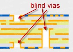
A blind via connects an outer layer of the PCB to one or more internal layers without extending through the entire board.
For example, a blind via may connect the top copper layer to the first internal signal layer. From the opposite side of the PCB, the via cannot be seen because it does not pass completely through the board.
Blind vias are particularly useful when a designer needs to connect surface-mounted components, such as fine-pitch BGAs, to internal routing layers while preserving valuable routing space on the remaining layers.
Blind vias may be produced using mechanical drilling or laser drilling, depending on the required dimensions, depth, aspect ratio, and HDI construction.
Advantages of Blind Vias
1. Higher routing density
Blind vias occupy fewer layers than conventional through-holes, leaving additional routing space available on internal layers.
2. Smaller PCB size
Because the via does not extend through the complete board, designers can optimize the stackup and reduce unnecessary routing restrictions.
3. Improved electrical performance
The shorter interconnection path can reduce via-related parasitic effects compared with long through-hole structures.
4. Better support for fine-pitch components
Blind vias are particularly useful for BGA, CSP, and other compact packages where conventional through-hole vias may interfere with routing.
Typical Applications
Blind vias are widely used in:
- Smartphones
- Tablets
- Wearable electronics
- Compact computing devices
- Automotive control modules
- Medical electronics
- High-density communication equipment
2. Buried Vias
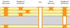
A buried via connects two or more internal PCB layers but does not extend to either external surface layer.
Because the structure is completely enclosed within the PCB stackup, it cannot be visually inspected from the top or bottom surface after fabrication.
Buried vias are generally formed within PCB cores or internal layer structures before subsequent lamination processes. This makes their manufacturing process more complex than conventional through-hole vias.
Buried vias are especially useful when internal routing requires additional interconnection flexibility without consuming valuable space on the external layers.
Advantages of Buried Vias
1. Efficient internal routing
Buried vias can connect internal signal layers without occupying space on the external component or routing layers.
2. Greater component-placement freedom
Because the via does not appear on the external surface, designers have more flexibility when positioning components and routing surface-level traces.
3. Higher routing density
Buried vias can be combined with blind vias and microvias to create sophisticated HDI stackups.
4. Suitable for complex multilayer designs
They are useful in high-density applications where conventional through-hole vias would consume too much routing area.
Disadvantages of Buried Vias
Higher manufacturing complexity
Buried vias often require additional drilling, plating, and lamination processes. IPC literature on HDI fabrication describes sequential lamination and buried-via processing as part of the advanced manufacturing techniques used to support high-density designs.
Higher PCB manufacturing cost
Additional fabrication steps can increase manufacturing time, process requirements, and overall cost.
More difficult troubleshooting
Because buried vias are hidden inside the PCB, visual inspection and physical troubleshooting can be more difficult than with exposed vias.
Typical Applications
Buried vias are commonly considered for:
- Medical equipment
- Industrial control systems
- Telecommunications hardware
- High-density computing equipment
- Automotive electronics
- Aerospace electronics
3. Microvias
A microvia is a very small blind-via structure that typically connects adjacent HDI layers.
IPC technical documentation commonly defines a microvia as a blind hole with a diameter of 150 μm (6 mil) or less, with associated pad dimensions also significantly smaller than conventional via structures.
Microvias are one of the defining technologies of modern HDI PCBs.
Unlike a conventional through-hole via that can pass through the entire PCB, a microvia normally spans only a single dielectric layer. This short vertical connection allows designers to place traces and vias much closer together.
Microvias are commonly manufactured using laser drilling, followed by copper metallization and other HDI processing steps.
Why Are Microvias Important?
Modern components such as BGAs and CSPs may have extremely small pitches. Conventional vias can be too large to fit efficiently between component pads.
Microvias solve this problem by providing much smaller interconnections.
They can be used to:
- Connect fine-pitch BGA pads
- Increase routing density
- Reduce via size
- Shorten signal paths
- Improve layer utilization
- Support compact PCB form factors
- Reduce unnecessary parasitic effects
IPC technical literature also notes that microvias can reduce inductance and capacitance compared with larger through-hole structures, contributing to improved electrical performance in high-density designs.
4. Stacked Microvias
A stacked microvia structure places two or more microvias vertically above one another.
For example, one microvia may connect Layer 1 to Layer 2, while another microvia directly underneath it connects Layer 2 to Layer 3.
The resulting structure creates a continuous vertical interconnection through multiple HDI build-up layers.
Stacked microvias are particularly useful when routing must pass through several HDI layers while maintaining a very small footprint.
Advantages of Stacked Microvias
Higher routing density
Stacked structures can provide a compact vertical connection between multiple layers.
Excellent space utilization
Because multiple microvias occupy approximately the same vertical footprint, they can support highly compact PCB layouts.
Shorter electrical paths
Microvias create short vertical transitions, which can be beneficial for high-speed and RF applications.
Useful for advanced component packaging
Stacked microvias are frequently considered when routing fine-pitch BGA and other high-density packages.
Thermal applications
Appropriately designed and filled microvia structures can also participate in thermal management, particularly in via-in-pad applications.
Disadvantages of Stacked Microvias
More complex manufacturing
Stacked structures require highly controlled drilling, metallization, alignment, and lamination processes.
Higher manufacturing cost
Additional processing and tighter tolerances can increase PCB Manufacturing costs.
Higher process sensitivity
Stacked microvias require precise registration and reliable copper interfaces between successive microvia levels.
Via filling may be required
Depending on the structure and application, copper-filled microvias may be required to create a reliable connection between stacked levels and to support planar via-in-pad construction. IPC documentation discusses via filling and planarization as important processes for HDI and microvia designs.
5. Staggered Microvias
A staggered microvia structure differs from a stacked structure because the microvias are laterally offset rather than positioned directly on top of one another.
For example, a microvia connecting Layer 1 to Layer 2 may be positioned slightly to the left of the microvia connecting Layer 2 to Layer 3.
This configuration can simplify certain manufacturing requirements because the vertical connections do not need to align perfectly through multiple levels.
Advantages of Staggered Microvias
1. Manufacturing flexibility
The lateral offset can reduce some of the manufacturing challenges associated with directly stacked microvias.
2. Lower structural complexity
Depending on the design and manufacturer, staggered structures may avoid some of the copper-filling requirements associated with stacked microvias.
3. Reliable HDI construction
When properly designed and manufactured, staggered microvias provide reliable connections between successive HDI layers.
4. Suitable for high-density routing
They provide additional routing options while still taking advantage of microvia technology.
Disadvantages of Staggered Microvias
More PCB area
Because each microvia is laterally offset, staggered structures generally require more horizontal space than directly stacked microvias.
More complicated routing
The offset geometry must be considered during breakout routing and layer transitions.
Potential signal-integrity considerations
For high-speed designs, every via transition should be evaluated as part of the complete transmission-line structure. Stackup, dielectric thickness, copper geometry, impedance, and return-current paths can all affect signal integrity.
Stacked vs. Staggered Microvias
The choice between stacked and staggered microvias is an important part of advanced PCB Design.
| Feature | Stacked Microvias | Staggered Microvias |
|---|---|---|
| Vertical alignment | Directly aligned | Laterally offset |
| PCB area | Very efficient | Requires more horizontal space |
| Manufacturing complexity | Higher | Generally lower |
| Copper filling | Often required depending on construction | May be reduced or avoided depending on design |
| Routing density | Very high | High |
| Alignment requirements | Very strict | Less demanding |
| Cost | Generally higher | Generally lower |
| Design flexibility | Excellent for compact layouts | Good for less constrained layouts |
| Typical use | Advanced HDI, fine-pitch BGA | High-density multilayer routing |
Neither structure is universally suitable for every application. The correct choice depends on the PCB stackup, routing density, component pitch, electrical requirements, manufacturing capabilities, and cost target.
Microvias vs. Blind Vias vs. Buried Vias
Although these terms are sometimes used interchangeably, they describe different characteristics.
| Via Type | Connection | Typical Manufacturing | Main Benefit |
|---|---|---|---|
| Through Via | Outer-to-outer through entire PCB | Mechanical drilling | Simple and economical |
| Blind Via | Outer layer to internal layer | Mechanical or laser drilling | Saves routing space |
| Buried Via | Internal layer to internal layer | Mechanical/laser + lamination | Maximizes internal routing |
| Microvia | Usually one HDI dielectric layer | Laser drilling | Very high density |
| Stacked Microvia | Multiple vertically aligned microvias | Laser drilling + plating/filling | Maximum space efficiency |
| Staggered Microvia | Multiple offset microvias | Laser drilling + plating | High density with less stacking complexity |
The important distinction is that microvia describes a size and construction category, while blind and buried describe where the via begins and ends within the PCB stackup.
Important HDI Via Design Parameters
Selecting a via structure requires more than simply choosing the smallest possible hole.
1. Via Diameter
Smaller vias allow higher routing density, but extremely small geometries require tighter manufacturing control.
IPC technical material identifies 150 μm (6 mil) as a commonly referenced microvia diameter limit.
However, actual manufacturing capability depends on the PCB manufacturer, material system, laser equipment, copper thickness, layer structure, and production volume.
2. Aspect Ratio
Aspect ratio is generally expressed as:
Aspect Ratio = Via Depth / Via Diameter
As the depth-to-diameter ratio increases, drilling, plating, and filling become more difficult.
For microvias, the relatively shallow depth is one reason laser drilling is practical.
3. Pad Size
The capture pad must provide sufficient area for reliable registration and connection.
A smaller pad increases routing density but also reduces manufacturing margin.
4. Annular Ring
The annular ring is the remaining copper area around the drilled hole.
Insufficient annular-ring dimensions can increase the risk of breakout or manufacturing defects.
Therefore, minimum annular-ring requirements should be established together with the PCB fabricator.
5. Via Filling
Via filling becomes especially important in high-density via-in-pad and stacked-microvia structures.
Proper filling and planarization can create a flat surface for component assembly and enable additional interconnection structures. IPC documentation identifies via filling and planarization as important techniques for HDI, microvia, and via-in-pad designs.
6. Sequential Lamination
Many HDI structures require sequential build-up processes rather than manufacturing the entire PCB stackup in a single lamination cycle.
This allows additional dielectric and copper layers to be built around the core structure.
7. Via-in-Pad
Via-in-pad places a via directly within a component pad.
This technique is particularly useful for fine-pitch BGA components because it eliminates the need to route every connection outward before transitioning to another layer.
For via-in-pad applications, the via may need to be filled and planarized to prevent solder from flowing into the via during assembly.
How to Choose the Right HDI Via Structure
Choosing the correct via structure should be based on the complete design rather than via size alone.
Step 1: Define the Component Pitch
Start with the smallest BGA, CSP, QFN, or other fine-pitch component on the board.
The component pitch often determines whether conventional vias can be used.
Step 2: Evaluate Routing Density
Determine how many signals must escape from each component and how many routing layers are available.
If conventional through-holes consume too much routing area, blind or microvia structures may be necessary.
Step 3: Define the PCB Stackup
The number of signal, power, and ground layers directly affects via selection.
The stackup should be designed together with impedance requirements and return-current paths.
Step 4: Consider Signal Integrity
For high-speed designs, evaluate:
- Via stub length
- Return-current path
- Parasitic capacitance
- Parasitic inductance
- Differential-pair transitions
- Impedance discontinuities
- Crosstalk
- Reference-plane continuity
Shorter via transitions can help reduce parasitic effects, but HDI alone does not automatically guarantee better signal integrity. Material selection, stackup, routing geometry, and grounding strategy remain critical.
Step 5: Evaluate Manufacturing Capability
Not every PCB manufacturer can produce the same HDI structures.
Before finalizing the design, confirm:
- Minimum laser-drilled hole size
- Minimum pad size
- Layer-to-layer registration
- Copper thickness
- Microvia aspect ratio
- Via filling capability
- Sequential lamination capability
- Minimum trace/space
- Via-in-pad capability
- Electrical testing requirements
Step 6: Optimize Cost
The smallest and most sophisticated via structure is not always the most economical solution.
A well-designed HDI PCB should balance:
Electrical Performance + Routing Density + Reliability + Manufacturing Capability + Cost
This balance is one of the most important principles of professional PCB Manufacturing.
HDI PCB Manufacturing Considerations
HDI manufacturing is considerably more process-sensitive than conventional multilayer PCB manufacturing.
A typical HDI production flow may involve:
- Material preparation
- Inner-layer imaging
- Inner-layer etching
- Inner-layer inspection
- Lamination
- Laser drilling
- Desmear and hole preparation
- Copper metallization
- Via filling when required
- Sequential build-up
- Additional imaging and etching
- Surface finishing
- Electrical testing
- AOI and other inspections
- Final quality inspection
The exact process varies according to the HDI construction, material system, number of build-up layers, via technology, and manufacturer’s process capabilities.
IPC documentation highlights sequential lamination, blind and buried vias, microvias, via filling, and planarization as important technologies associated with high-density PCB fabrication.
For this reason, designers should involve the PCB manufacturer early in the development process rather than designing the board first and checking manufacturability afterward.
Common HDI PCB Design Mistakes
Mistake 1: Making Vias Smaller Without Checking Manufacturing Capability
A smaller via does not automatically mean a better PCB.
If the manufacturer cannot reliably fabricate the specified structure, yield and reliability may suffer.
Mistake 2: Ignoring Stackup Design
Via geometry and stackup design are closely related.
A poorly planned stackup can create impedance discontinuities, long signal transitions, and difficult return-current paths.
Mistake 3: Using Stacked Microvias Everywhere
Stacked microvias provide excellent space efficiency but can increase manufacturing complexity and cost.
Use them where their space-saving benefits justify the additional processing requirements.
Mistake 4: Failing to Consider Via Filling
Via filling can be essential for some stacked and via-in-pad structures.
The filling process should be included in the design and manufacturing discussion from the beginning.
Mistake 5: Designing Without DFM Review
A PCB may appear electrically correct in CAD software but still be difficult or expensive to manufacture.
A professional DFM review can identify issues involving:
- Hole size
- Pad size
- Copper clearance
- Layer registration
- Trace width
- Trace spacing
- Via density
- Aspect ratio
- Annular ring
- Via filling
- Lamination structures
Why HDI Vias Matter for Modern Electronics
The continued miniaturization of electronic products is making conventional PCB interconnection structures increasingly restrictive.
Microvias and advanced HDI structures provide several important benefits:
- Higher wiring density
- Smaller PCB dimensions
- Better utilization of PCB layers
- Support for fine-pitch components
- Shorter interconnect paths
- Greater design flexibility
- Potentially improved high-speed electrical performance
- Better support for compact electronic products
IPC technical studies have described microvia technology as an important approach for accommodating smaller and faster devices while improving interconnection density and addressing signal-integrity challenges.
Final Thoughts
HDI PCB technology has become an important solution for modern electronic products that require compact dimensions, high component density, and increasingly demanding electrical performance.
Blind vias, buried vias, and microvias each provide different interconnection capabilities. Stacked microvias maximize vertical space utilization, while staggered microvias can provide a practical alternative when manufacturing complexity and cost need to be controlled.
The best HDI structure is not necessarily the smallest or most advanced option. A successful design must consider component pitch, routing density, PCB stackup, signal integrity, aspect ratio, via filling, sequential lamination, manufacturing tolerances, reliability, and total cost.
For engineers working on advanced PCB Design projects, early collaboration with an experienced PCB Manufacturing partner is essential. Kingda can evaluate the complete PCB structure, manufacturing requirements, and DFM considerations to help ensure that complex HDI designs can be translated into reliable, manufacturable circuit boards.
Ultimately, successful HDI development depends on balancing miniaturization, electrical performance, manufacturing capability, and long-term reliability rather than optimizing a single design parameter.