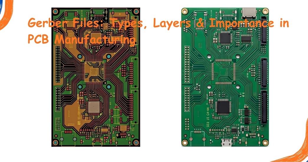
Gerber Files for PCB Manufacturing: Formats, Layers, Generation & DFM Checklist
Gerber files are one of the most important data formats used to transfer PCB design information from CAD software to a PCB manufacturer. They contain the graphical data required to fabricate individual PCB layers, including copper patterns, solder mask, silkscreen, board outlines, and other manufacturing features.
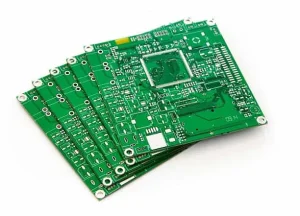
For many PCB projects, the Gerber package works together with NC drill data and manufacturing documentation to provide the information required to fabricate the bare printed circuit board. If these files are incomplete, incorrectly configured, or inconsistent with the original design, the manufacturer may not be able to produce the intended PCB accurately.
For PCB designers, hardware engineers, and electronics manufacturers, understanding the Gerber file format is essential for preventing manufacturing errors, reducing engineering questions, and improving production efficiency.
This guide explains what Gerber files are, how they are structured, what information they contain, the most common Gerber file types and extensions, the differences between Gerber X1/X2/X3, how to generate Gerber files, common export mistakes, and the final DFM checklist that should be completed before sending PCB manufacturing data to a supplier.
What Is a Gerber File?
A Gerber file is a standardized format for transferring PCB image data from a design system to PCB manufacturing equipment and CAM software.
Gerber is widely regarded as the de facto standard for PCB design-to-manufacturing data exchange. Modern Gerber files can describe individual PCB layers such as copper, solder mask, and legend, while attributes can provide additional information about the function of files and features.
A PCB design is normally not transferred as one single Gerber file.
Instead, each manufacturing layer is represented by a separate file.
For example, a simple two-layer PCB may include:
- Top copper
- Bottom copper
- Top solder mask
- Bottom solder mask
- Top silkscreen
- Bottom silkscreen
- Board outline
- NC drill data
A more complex multilayer PCB will contain additional Gerber files for each internal copper layer.
The Gerber files describe the two-dimensional geometry of the PCB. Other manufacturing information, such as finished board thickness, material, copper weight, surface finish, impedance requirements, tolerances, and special fabrication instructions, may be provided separately or through additional standardized manufacturing documentation.
Why Are Gerber Files Important?
Gerber files form a critical bridge between PCB Design and PCB Manufacturing.
A PCB CAD system may contain many types of design information, including:
- Schematic relationships
- Component libraries
- Net names
- Component properties
- Design rules
- 3D models
- Manufacturing constraints
- Routing information
However, a PCB fabricator does not simply manufacture the board directly from the designer’s CAD project file.
The manufacturer needs a fabrication data package that can be interpreted by CAM systems and manufacturing equipment.
Gerber data provides the graphical layer information required to reproduce the physical PCB geometry.
Ucamco describes Gerber as the backbone of electronics fabrication and notes that PCB design systems can output Gerber data while PCB fabrication software can process it.
What Information Is Stored in Gerber Files?
A typical Gerber fabrication package may contain graphical information representing:
- Copper traces
- Copper pads
- Copper planes
- Solder mask openings
- Silkscreen graphics
- Board outlines
- Slots and routed features
- Other fabrication-layer graphics
Drill information is commonly supplied separately as NC drill data, although modern Gerber-related workflows can also represent drill and route information.
A complete manufacturing package may therefore include both Gerber layer files and drill data, together with fabrication drawings and other manufacturing specifications.
Gerber File Structure
A Gerber file is more than a simple picture of a PCB layer. It is a machine-readable description of two-dimensional graphics.
Understanding its basic structure helps PCB designers identify export problems before manufacturing.
1. Header Information
The header can contain important information such as:
- Units
- Coordinate format
- Image polarity
- Aperture definitions
- Other format parameters
- Attributes, depending on the Gerber version
Modern Extended Gerber includes aperture definitions within the file, eliminating the dependency on the separate aperture files associated with older workflows.
2. Coordinate Data
Coordinate commands define where graphical features are located.
These coordinates can describe:
- Lines
- Arcs
- Pads
- Flashes
- Polygons
- Board geometry
The manufacturing system uses these coordinates to reconstruct the intended PCB layer.
3. Aperture Definitions
An aperture defines the shape used to create graphical features.
Depending on the design, an aperture may represent shapes used for:
- Tracks
- Pads
- Lines
- Flashes
- Filled regions
Modern Gerber embeds aperture definitions within the file, which helps make the data more self-contained.
4. Drawing Commands
Gerber commands determine how graphical features are created.
The data can specify operations such as:
- Move
- Draw
- Flash
- Region fill
When combined with coordinate and aperture information, these commands allow the PCB layer to be reproduced accurately.
Gerber File Layers Explained
A PCB consists of multiple physical and manufacturing layers, each serving a different purpose.
A complete Gerber package separates these layers so that the PCB manufacturer can process them individually.
Copper Layers
Copper Gerber files define conductive features such as:
- Traces
- Pads
- Copper pours
- Planes
- Other copper geometries
A two-layer PCB normally has one top copper layer and one bottom copper layer.
A multilayer PCB has separate data for each internal copper layer.
Solder Mask Layers
Solder mask files define where solder mask is present or where openings are required.
Typical files include:
- Top solder mask
- Bottom solder mask
The openings expose copper pads and other areas that need to remain accessible during soldering.
Solder mask design is especially important for fine-pitch components because incorrect mask openings can affect solderability and assembly yield.
Silkscreen Layers
Silkscreen, also called legend, contains non-conductive markings such as:
- Reference designators
- Component outlines
- Polarity indicators
- Pin-1 indicators
- Logos
- Assembly instructions
- Identification markings
Silkscreen improves assembly, inspection, troubleshooting, and maintenance.
Typical files include:
- Top silkscreen
- Bottom silkscreen
Board Outline and Mechanical Data
The board outline defines the physical shape and finished dimensions of the PCB.
Depending on the CAD system and manufacturing workflow, the outline may be supplied in a dedicated mechanical or profile layer.
It can include:
- Board perimeter
- Slots
- Cutouts
- Routed features
- Internal mechanical openings
The board outline is critical because it determines the physical dimensions of the finished board.
NC Drill Data
Drill data defines the location and size of holes required for PCB fabrication.
These may include:
- Plated through holes
- Non-plated through holes
- Via holes
- Mounting holes
- Component holes
- Slots, depending on the manufacturing format
Drill data is normally supplied separately from the Gerber image files in conventional fabrication packages.
Common Gerber Files and Extensions
File extensions vary between PCB design tools and manufacturing workflows, so designers should not rely solely on the extension to determine the layer function.
Common extensions include:
| PCB Layer / Data | Typical Extension | Purpose |
|---|---|---|
| Top Copper | .GTL |
Top copper traces, pads, and planes |
| Bottom Copper | .GBL |
Bottom copper features |
| Internal Copper | .G1, .G2, .G3… |
Internal signal or plane layers |
| Top Solder Mask | .GTS |
Top solder mask openings |
| Bottom Solder Mask | .GBS |
Bottom solder mask openings |
| Top Silkscreen | .GTO |
Top component markings and legend |
| Bottom Silkscreen | .GBO |
Bottom component markings and legend |
| Board Outline | .GKO, .GM1, or other CAD-specific output |
Board profile and mechanical geometry |
| Top Solder Paste | .GTP |
Top stencil/paste openings |
| Bottom Solder Paste | .GBP |
Bottom stencil/paste openings |
| NC Drill | .DRL, .TXT, or manufacturer-specific |
Hole sizes and locations |
| Drill Drawing | .PDF or CAD-specific |
Visual reference for drill information |
These extensions are conventions rather than universal requirements. The actual file naming scheme depends on the PCB CAD system and the manufacturer’s CAM workflow.
Gerber File Formats: X1, X2, and X3
Gerber has evolved significantly over time.
The most important distinction for modern PCB manufacturing is between conventional Extended Gerber data and Gerber with attributes.
Gerber X1
X1 refers to Extended Gerber without the newer X2 attributes.
It provides the graphical description of the PCB layer but does not provide the same standardized layer and feature metadata available through X2 attributes.
Gerber X2
Gerber X2 extends the Gerber format by adding standardized attributes.
Ucamco explains that X2 is essentially Extended Gerber with attributes and remains backward compatible with the underlying Gerber image data.
These attributes can identify information such as:
- File function
- File polarity
- PCB panel or part information
- Pad function
- SMD pad
- Via pad
- Fiducial
This additional information helps communicate design intent from CAD to CAM more clearly.
For modern PCB Manufacturing, X2 can reduce ambiguity during CAM preparation.
Gerber X3
Gerber X3 extends the Gerber ecosystem further toward assembly-related data.
It is designed to carry additional information associated with PCB assembly and components.
However, X3 should not be described as simply a universally adopted replacement for X2. Manufacturing and assembly workflows vary, and support depends on the CAD/CAM systems used by the designer and manufacturer.
Ucamco currently provides X3 specifications and test files as part of the Gerber ecosystem.
For most standard PCB fabrication projects, designers should follow the manufacturer’s requested Gerber version and data package requirements rather than selecting a format solely because it is newer.
How to Generate Gerber Files
Generating Gerber files is usually one of the final steps before sending a PCB to manufacturing.
Most modern PCB CAD tools provide built-in Gerber export functions.
However, simply clicking “Export” does not guarantee that the manufacturing package is correct.
Step 1: Complete the PCB Design
Before generating manufacturing files, confirm that:
- The schematic is complete
- PCB placement is finalized
- Routing is complete
- Component footprints are correct
- Design rules have been checked
- Copper zones are properly filled
- Board dimensions are correct
Run both electrical and design-rule checks where applicable.
Step 2: Review the Stackup
For multilayer PCBs, confirm:
- Layer count
- Copper weight
- Dielectric thickness
- Core and prepreg structure
- Finished board thickness
- Controlled-impedance requirements
The Gerber files should correspond to the final approved stackup.
Step 3: Configure Gerber Output
In the PCB CAD software, select the required fabrication layers.
Typical outputs include:
- Top copper
- Bottom copper
- Internal copper
- Top solder mask
- Bottom solder mask
- Top silkscreen
- Bottom silkscreen
- Board outline
Select the appropriate units and coordinate settings according to the CAD system and manufacturer requirements.
Step 4: Generate NC Drill Files
Generate the required NC drill data separately.
Verify:
- Drill sizes
- Hole coordinates
- Plated vs. non-plated holes
- Tool definitions
- Slots, if applicable
For advanced HDI boards, additional manufacturing data may be required depending on the via structure and manufacturer’s process.
Step 5: Generate Fabrication Documentation
A manufacturing drawing can communicate information that cannot be inferred reliably from layer images alone.
Depending on the project, include:
- Board thickness
- Copper weight
- Surface finish
- Material
- Tolerances
- Impedance requirements
- Special fabrication instructions
- Via requirements
- Surface-finish requirements
Step 6: Review the Gerber Package
Open the actual exported files in a Gerber viewer rather than relying only on the PCB CAD preview.
Check every layer independently and then inspect the complete layer stack.
How to Check Gerber Files Before Manufacturing
A Gerber review should be performed before the files are released to the PCB manufacturer.
Check 1: Verify Layer Count
Make sure the number of exported copper layers matches the intended PCB stackup.
For example, a six-layer PCB should contain:
- Top copper
- Four internal copper layers
- Bottom copper
unless the manufacturer’s data structure uses another explicit representation.
Check 2: Verify Layer Order
Confirm that the correct copper data corresponds to the correct physical layer.
An incorrectly assigned internal layer can cause serious manufacturing problems.
Check 3: Check Copper Geometry
Inspect:
- Trace width
- Pad dimensions
- Copper pours
- Clearances
- Thermal reliefs
- Copper-to-edge clearance
Check 4: Check Solder Mask
Verify that solder mask openings are correctly aligned with:
- SMD pads
- Through-hole pads
- Via structures
- Exposed copper areas
Check 5: Check Silkscreen
Make sure silkscreen does not overlap solderable pads or critical exposed copper areas.
Check:
- Reference designators
- Polarity marks
- Component outlines
- Pin-1 indicators
- Logos
Check 6: Check Drill Alignment
Overlay the NC drill data with the copper layers.
Verify that:
- Vias align with pads
- Through holes align with pads
- Mounting holes are correctly positioned
- Drill sizes are correct
- Slots are correctly represented
Check 7: Check Board Outline
The board outline should form a clear and unambiguous profile.
Check:
- Overall dimensions
- Corner geometry
- Cutouts
- Slots
- Internal openings
- Routed areas
Check 8: Compare With the Original PCB Design
The final Gerber package should be compared against the original CAD layout.
This step can identify export problems that may not be obvious when looking at individual files.
Common Gerber File Mistakes
Even when the original PCB layout is correct, manufacturing problems can occur if the exported Gerber package is incomplete or inconsistent.
1. Missing Manufacturing Layers
A common problem is failing to export one or more required layers.
Potentially missing data includes:
- Internal copper
- Solder mask
- Silkscreen
- Board outline
- Drill data
2. Incorrect Layer Assignment
A file may be exported correctly but assigned to the wrong physical layer.
This can be particularly dangerous in multilayer PCBs.
3. Incorrect Board Outline
If the board profile is incomplete or ambiguous, the manufacturer may not know the exact finished-board dimensions.
The profile should clearly define the PCB perimeter and any required cutouts or slots.
4. Drill Data Misalignment
If the drill file uses a different origin or coordinate system from the Gerber data, holes may not align with pads.
Always inspect drill data together with the copper layers.
5. Incorrect Polarity
Positive and negative layers must be interpreted correctly.
Incorrect polarity can completely change the intended copper or solder-mask geometry.
6. Unfilled Copper Zones
Some CAD systems require copper zones to be repoured before manufacturing output.
If the exported copper layer does not contain the intended copper fill, the manufactured PCB may differ from the design.
7. Incorrect Solder Mask Expansion
Incorrect mask expansion can result in:
- Pads being partially covered
- Excessive exposed copper
- Solder bridges
- Poor solderability
8. Silkscreen Over Pads
Silkscreen overlapping solderable areas may interfere with assembly.
This should be checked before production.
9. Missing Fabrication Specifications
Gerber files alone may not communicate every manufacturing requirement.
Information such as:
- Finished thickness
- Copper weight
- Material
- Surface finish
- Impedance
- Tolerances
may need to be supplied through fabrication drawings, stackup documentation, or other manufacturing data.
Gerber vs. ODB++ vs. IPC-2581
Gerber is not the only PCB manufacturing data format.
Modern PCB workflows may also use ODB++ and IPC-2581.
Gerber
Gerber primarily represents PCB layer and manufacturing geometry, with X2/X3 attributes providing additional metadata.
Advantages:
- Very widely supported
- Simple layer-based structure
- Mature ecosystem
- Easy to inspect
- Supported by most PCB CAM systems
ODB++
ODB++ is a structured manufacturing data format designed to represent PCB design and manufacturing information in a more integrated form.
It can package more information than a conventional collection of independent Gerber layers.
IPC-2581
IPC-2581 is an open standard for exchanging PCB manufacturing, assembly, and inspection information.
IPC describes IPC-2581 as an XML-based intelligent data format capable of representing information needed for tooling, manufacturing, assembly, and inspection.
IPC materials also identify Gerber, ODB++, and GenCAM/IPC-2581 as formats used in PCB manufacturing data exchange.
Comparison
| Feature | Gerber | ODB++ | IPC-2581 |
|---|---|---|---|
| Layer geometry | Excellent | Yes | Yes |
| Manufacturing metadata | Available through attributes/additional data | Extensive | Extensive |
| Individual layer files | Usually yes | Integrated structure | Integrated structure |
| Netlist information | Not inherently part of basic Gerber image data | Supported | Supported |
| BOM/assembly information | Limited/not part of basic layer data | Supported | Supported |
| Industry maturity | Very high | High | Growing adoption |
| CAM compatibility | Excellent | High | Increasing |
| Best suited for | Broad PCB fabrication workflows | Integrated manufacturing data | Integrated fabrication/assembly/inspection data |
There is no requirement that every project use the newest data format. The correct choice depends on the CAD system, CAM system, manufacturer, assembly provider, and project requirements.
Gerber Files vs. PCB Design Files
A common misunderstanding is that a Gerber package is simply another version of the original PCB CAD file.
It is not.
A PCB design file may contain:
- Schematic information
- Component libraries
- Component properties
- Net names
- Design rules
- Routing
- 3D models
- Manufacturing settings
A Gerber package primarily communicates the physical graphical information needed to fabricate PCB layers.
Therefore, the manufacturer generally should not be expected to reconstruct the designer’s complete CAD environment from Gerber files alone.
For advanced projects, additional information such as:
- NC drill files
- Fabrication drawing
- Stackup
- Impedance requirements
- Material specifications
- Assembly drawings
- BOM
- Pick-and-place files
may be necessary.
Gerber DFM Checklist Before PCB Manufacturing
Before sending the manufacturing package to a PCB supplier, complete the following checklist.
Design Verification
- Schematic finalized
- PCB layout finalized
- DRC completed
- ERC completed where applicable
- Copper zones repoured
- Component footprints verified
- Board dimensions confirmed
Gerber Verification
- Top copper checked
- Bottom copper checked
- All internal copper layers checked
- Top solder mask checked
- Bottom solder mask checked
- Top silkscreen checked
- Bottom silkscreen checked
- Board outline checked
Drill Verification
- NC drill file included
- Drill sizes verified
- Plated holes verified
- Non-plated holes verified
- Slots checked
- Drill-to-pad alignment verified
Manufacturing Specification
- Layer count confirmed
- Board thickness confirmed
- Copper thickness confirmed
- Material confirmed
- Surface finish confirmed
- Solder mask color confirmed
- Silkscreen color confirmed
- Impedance requirements confirmed
- Dimensional tolerances confirmed
Final CAM Review
- Gerber files opened in a viewer
- All layers visually inspected
- Drill files overlaid
- Board outline verified
- Layer polarity verified
- Manufacturing package compared with the original PCB design
Best Practices for Gerber File Preparation
To make the transition from PCB Design to PCB Manufacturing more efficient, follow these practices:
Use Consistent File Naming
Use clear names such as:
Project.GTLProject.GBLProject.GTSProject.GBSProject.GTOProject.GBOProject.G1Project.G2Project.DRL
Avoid ambiguous file names that force the manufacturer to interpret the intended layer.
Include a Readme or Fabrication Drawing
For complex boards, provide a fabrication drawing or manufacturing note containing:
- Board dimensions
- Layer count
- Finished thickness
- Copper weight
- Surface finish
- Material
- Special tolerances
- Impedance requirements
- Special manufacturing instructions
Use the Manufacturer’s Capabilities
Do not design solely according to theoretical minimum values.
Instead, compare the design with the actual capabilities of your selected PCB manufacturer.
For example:
- Minimum trace width
- Minimum spacing
- Minimum drill size
- Minimum annular ring
- Maximum aspect ratio
- Copper thickness
- Surface finish capability
Archive the Exact Released Data
Once the Gerber package has been approved for production, archive the exact manufacturing package.
This makes it easier to:
- Reorder the PCB
- Compare revisions
- Investigate manufacturing issues
- Maintain product traceability
- Prevent accidental production from outdated files
Conclusion
Gerber files remain a fundamental part of modern PCB Manufacturing because they provide a standardized way to transfer PCB layer geometry from design systems to manufacturing systems.
A complete Gerber package can describe the copper layers, solder mask, silkscreen, board profile, and other fabrication geometries, while NC drill data provides the hole information required for drilling. Modern Gerber X2 adds standardized attributes that communicate layer and feature information more clearly, while X3 extends the ecosystem toward additional assembly-related data.
However, generating Gerber files is only one step in preparing a PCB for production.
A reliable manufacturing package should also include appropriate drill data, fabrication documentation, stackup information, material requirements, surface-finish specifications, impedance requirements, and other project-specific manufacturing instructions.
Before production, designers should always open the actual exported files in a Gerber viewer and verify every layer, drill location, board outline, solder-mask opening, silkscreen feature, and copper geometry.
For complex multilayer, HDI, high-speed, and fine-pitch PCB projects, a professional DFM review is equally important. A PCB that passes CAD design-rule checks may still require manufacturing adjustments based on the selected fabricator’s actual process capabilities.
Kingda can review PCB manufacturing data, perform DFM analysis, evaluate Gerber and drill files, and help ensure that the transition from PCB Design to PCB Manufacturing is accurate, efficient, and suitable for production.