Prepreg PCB Structure: PCB Design, PCB Manufacturing & Multilayer PCB Guide
The electronics industry continuously faces the challenge of developing devices that are compact, multifunctional, thermally stable, and capable of operating at high speeds. These design objectives must also be balanced against manufacturing costs. As a result, PCB designers and engineers must carefully define product requirements and make trade-offs among electrical performance, mechanical structure, thermal management, manufacturability, and cost.
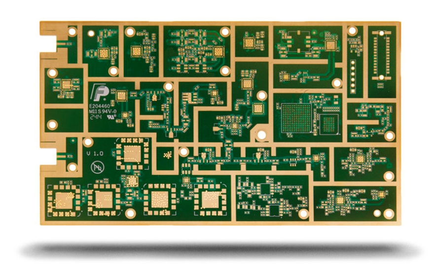
A printed circuit board (PCB) is a critical component of many electronic systems. It mechanically supports electronic components while providing conductive pathways that connect them and enable the intended electrical functions.
Depending on the requirements of the final product, PCBs can be manufactured in single-layer, double-layer, and multilayer configurations. As the number of conductive layers increases, the PCB generally becomes more complex and may require additional manufacturing processes. For example, a board with conductive copper layers on both sides of a dielectric core is classified as a double-sided PCB.
When a multilayer PCB is cut through its thickness, its cross-section reveals a carefully engineered stackup consisting primarily of copper layers, dielectric materials, and resin systems. Among these materials, PCB prepreg plays an important role because it bonds individual layers together while providing electrical insulation and helping determine the final thickness and dielectric characteristics of the board.
This article explains the basic structure of prepreg-based multilayer PCBs, the functions of prepreg, core materials, and copper foil, and the major steps involved in PCB Manufacturing.
What Is a Multilayer PCB?
A multilayer PCB consists of multiple conductive copper layers separated by dielectric materials. Unlike a single-sided or double-sided PCB, a multilayer board contains internal copper layers in addition to its outer conductive layers.
The number of layers depends on the electrical, mechanical, thermal, and routing requirements of the application. Common configurations include 4-layer, 6-layer, 8-layer, and higher-layer-count boards. Advanced designs can contain many more layers, although increasing the layer count generally increases material consumption, fabrication complexity, lamination cycles, inspection requirements, and overall cost.
In practical PCB Design, the layer count should therefore be selected according to actual routing density, signal-integrity requirements, power distribution, thermal management, and mechanical constraints rather than simply maximizing the number of layers.
A typical rigid multilayer PCB may contain several copper-clad cores combined with multiple prepreg layers. During lamination, the prepreg softens, flows, and cures to bond adjacent layers into a mechanically stable structure.
Flexible and rigid-flex PCBs use different material systems and construction methods. Flexible circuits generally rely on polyimide-based dielectric materials rather than conventional FR-4 systems, although adhesive and adhesive-less constructions are both available depending on the application.
PCB prepreg styles such as 1080 and 2116 are commonly used in multilayer PCB fabrication. Their final contribution to the stackup depends not only on the nominal glass style but also on resin content, copper pattern coverage, lamination pressure, temperature, and the manufacturer’s process conditions.
Three Basic Elements of a Multilayer PCB
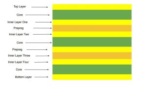
A multilayer PCB can be understood by examining three fundamental material categories: PCB prepreg, core material, and copper foil.
Together, these materials determine the board’s electrical insulation, mechanical strength, layer-to-layer bonding, copper connectivity, dielectric thickness, and overall stackup.
1. PCB Prepreg
PCB prepreg is a composite dielectric material made primarily from woven glass fiber impregnated with partially cured resin. It does not normally contain copper foil itself.
During multilayer lamination, heat and pressure cause the resin in the prepreg to soften and flow. The resin fills microscopic gaps between adjacent layers and then cures, creating a solid dielectric structure that bonds the layers together.
Prepreg therefore performs several important functions:
- Bonds adjacent PCB layers together
- Provides electrical insulation between copper layers
- Controls dielectric spacing within the stackup
- Contributes to the overall board thickness
- Helps determine impedance characteristics
- Provides mechanical support after curing
FR-4-based prepreg is widely used in conventional rigid multilayer PCBs because of its established electrical, mechanical, thermal, and manufacturing properties.
Prepreg is available in different glass styles and resin contents. Common glass styles include 1080, 2116, and other constructions. The final dielectric thickness after lamination is not necessarily identical to the dry prepreg thickness because resin flow and compression occur during the lamination process.
For this reason, PCB manufacturers such as Kingda typically select prepreg combinations according to the complete stackup rather than treating each prepreg style as an independent fixed-thickness material.
Resin content is another important consideration. Higher-resin-content materials can provide greater resin flow and may be useful for filling certain copper topographies, but they can also influence dielectric thickness, dimensional stability, and lamination behavior.
Therefore, selecting the correct prepreg is an important part of high-quality PCB Design and PCB Manufacturing.
2. Core Material
The core is a rigid dielectric laminate with copper foil already bonded to one or both sides. In a multilayer PCB, one or more cores can be combined with prepreg during the lamination process.
A typical core consists of:
- Copper foil
- Fiberglass reinforcement
- Cured resin system
Unlike prepreg, the resin in a conventional core has already been fully cured before the multilayer lamination stage.
The core plays an important role in determining the mechanical structure and electrical characteristics of the PCB. Its thickness, dielectric constant, loss characteristics, copper thickness, and dimensional stability can all affect the final board.
Depending on the stackup, different cores can serve as signal, power, or ground-layer structures. High-speed designs may require carefully controlled dielectric thicknesses and material properties to achieve the desired controlled impedance.
A multilayer PCB may therefore contain multiple core materials separated by prepreg layers. This construction is particularly important when designing high-density or high-speed boards where layer-to-layer spacing must be tightly controlled.
3. Copper Foil
Copper is the primary conductive material used in conventional PCBs. Copper foil forms the conductive layers that eventually become traces, planes, pads, and other electrical structures.
Copper foil selection depends on several factors, including:
- Copper thickness
- Current-carrying requirements
- Trace width and spacing
- Thermal requirements
- Mechanical requirements
- Surface treatment
- Manufacturing capability
Standard copper thicknesses are commonly specified in ounces per square foot, although PCB manufacturers also use micrometers or mils when defining copper thickness.
For example, 1 oz copper is approximately 35 µm thick before processing. Heavier copper may be selected for power electronics, automotive systems, battery-management systems, industrial equipment, and other applications requiring higher current capacity.
Copper foil also requires suitable surface treatment and bonding characteristics so that it maintains reliable adhesion to the dielectric material throughout PCB fabrication and subsequent operation.
In high-reliability applications, copper surface profile and treatment can also influence high-frequency signal loss, adhesion, etching behavior, and manufacturing consistency.
How Are Multilayer PCBs Manufactured?
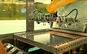
After understanding the roles of prepreg, core materials, and copper foil, the next step is to examine how these materials are converted into a finished multilayer circuit board.
The PCB Manufacturing process involves multiple tightly controlled operations. Depending on the board structure, technology, and manufacturer, the exact process flow can vary.
1. Multilayer Stackup and Sequential Lamination
Multilayer PCB fabrication begins with the design of the layer stackup.
The manufacturer determines the combination of:
- Core materials
- Prepreg materials
- Copper foil
- Dielectric thickness
- Copper weights
- Signal layers
- Power planes
- Ground planes
The internal circuit layers are typically fabricated and patterned before the multilayer lamination process.
During lamination, heat and pressure cause the prepreg resin to flow and cure, bonding the individual layers into a single multilayer panel.
For advanced HDI constructions, sequential lamination may be required to create additional buildup layers and microvia structures.
The number of lamination cycles directly affects production time and process complexity. Multiple lamination cycles also increase the importance of dimensional registration, material compatibility, resin flow control, and thermal expansion management.
The coefficient of thermal expansion (CTE) of the materials must be considered carefully, especially for multilayer and high-reliability PCBs. Excessive mismatch in material expansion can contribute to mechanical stress and reliability problems during thermal cycling.
2. Drilling and Plating
After lamination, the panel undergoes drilling according to the manufacturing data.
CNC mechanical drilling is widely used for conventional through-holes, while laser drilling can be used for microvias and certain HDI structures.
Drilling must be accurately controlled because hole diameter, location, aspect ratio, and positional tolerance directly influence PCB reliability and manufacturability.
After drilling, the panels undergo desmear and hole-wall preparation processes as required. Copper plating is then used to metallize the hole walls and establish electrical connections between the appropriate conductive layers.
For high-density multilayer PCBs, accurate registration between drilled holes and internal copper features is particularly important.
3. Circuit Pattern Formation and Etching
The copper layers are processed to create the required circuit patterns.
Depending on the manufacturing method, this may involve photoresist coating, exposure, development, copper plating, and etching.
During etching, unwanted copper is removed while the protected areas remain as conductive traces and planes.
Fine-line PCB designs require tight control over exposure, development, etching compensation, copper thickness, and dimensional accuracy.
This is especially important for advanced PCB Design applications with fine-pitch components, narrow traces, and high routing density.
4. Solder Mask Application
A solder mask is applied to protect exposed copper and reduce the risk of solder bridging between adjacent conductive features.
Liquid photoimageable solder mask (LPI) is widely used in modern PCB manufacturing. The general process includes coating, drying, exposure, development, and curing.
The solder mask also contributes to the visual appearance of the finished board. Green is the most widely recognized solder mask color, although black, blue, red, white, yellow, and other colors are available for specific applications.
For fine-pitch PCB assemblies, solder mask registration and opening accuracy are particularly important because poorly controlled openings can affect solderability and assembly yield.
5. Surface Finish
Exposed copper surfaces generally require a suitable surface finish to improve solderability and protect the copper from oxidation and contamination.
Common PCB surface finishes include:
- ENIG (Electroless Nickel Immersion Gold)
- HASL (Hot Air Solder Leveling)
- Lead-free HASL
- Immersion Silver
- Immersion Tin
- ENEPIG
The appropriate finish depends on component pitch, storage requirements, soldering process, electrical performance, cost, and reliability requirements.
For example, ENIG is commonly selected for fine-pitch applications because it provides a relatively flat surface. HASL can be cost-effective for many conventional applications, while other finishes may be selected for specific environmental, electrical, or assembly requirements.
Therefore, surface finish selection should be considered during both PCB Design and manufacturing planning.
6. Silkscreen and Identification Marking
Silkscreen, also known as the legend layer, provides useful visual information on the PCB.
Typical markings include:
- Component reference designators
- Polarity indicators
- Connector labels
- Pin-1 indicators
- Manufacturer information
- Revision information
- Traceability codes
These markings help operators and technicians identify components during PCB assembly, inspection, repair, and maintenance.
Modern PCB production may use screen printing or other direct-printing technologies depending on the required resolution and manufacturing process.
7. Inspection and Electrical Testing
Inspection and testing are essential for ensuring that the finished PCB meets the required design and manufacturing specifications.
Automated optical inspection (AOI) can identify many visual and pattern-related defects, including missing or excess copper features, incorrect patterns, and certain dimensional problems.
Electrical testing can be performed using methods such as:
- Flying probe testing
- Fixture-based electrical testing
- In-circuit testing (ICT), where applicable
- Other specialized electrical verification methods
The appropriate test method depends on the product volume, board complexity, test coverage requirements, and manufacturing stage.
For high-reliability applications, additional inspections such as dimensional inspection, microsection analysis, solderability testing, impedance testing, or other qualification tests may also be required.
Why Is Prepreg Selection Important in PCB Design?
Prepreg selection is not simply a material purchasing decision. It directly affects the electrical and mechanical performance of a multilayer PCB.
Important parameters include:
Dielectric Thickness
The thickness between copper layers influences controlled impedance, capacitance, signal propagation, and overall board thickness.
Resin Content
Resin content affects flow characteristics, final dielectric thickness, and the ability of the material to fill spaces between copper features.
Glass Style
Different glass styles have different constructions and resin distributions. They can influence dielectric uniformity and high-speed signal behavior.
Thermal Expansion
Material CTE affects dimensional stability and reliability during lamination, soldering, and thermal cycling.
Dielectric Properties
For high-speed and RF applications, dielectric constant (Dk) and dissipation factor (Df) must be considered because they affect signal propagation and insertion loss.
Consequently, engineers should define the complete PCB stackup early in the design process instead of selecting prepreg materials only after routing has been completed.
Common Multilayer PCB Stackup Considerations
A typical multilayer PCB stackup may include:
| Layer/Material | Primary Function |
|---|---|
| Top Copper | Components, signals, pads |
| Prepreg | Insulation and layer bonding |
| Internal Copper | Signal, power, or ground |
| Core | Structural dielectric and copper support |
| Prepreg | Insulation and bonding |
| Bottom Copper | Signals, components, and pads |
The exact arrangement depends on the PCB’s electrical and mechanical requirements.
For high-speed boards, designers often use dedicated reference planes adjacent to critical signal layers. This can help control impedance and provide a predictable return-current path.
For power electronics, the stackup may prioritize copper thickness, current capacity, thermal performance, and mechanical reliability.
For HDI designs, sequential buildup layers and microvias can be incorporated into the stackup to support fine-pitch components and high routing density.
Prepreg vs. Core: What Is the Difference?
Although prepreg and core materials are both dielectric components, they perform different functions during PCB fabrication.
| Feature | PCB Prepreg | PCB Core |
|---|---|---|
| Resin state before lamination | Partially cured | Fully cured |
| Copper foil | Typically supplied without copper | Copper-clad |
| Primary function | Bonding and insulation | Structural dielectric and conductive-layer support |
| Processing | Flows and cures during lamination | Maintains its basic structure |
| Stackup role | Bonds adjacent layers | Forms rigid dielectric sections |
| Thickness after lamination | Depends on resin flow and compression | Relatively stable |
Understanding this distinction is important when developing a manufacturable multilayer PCB stackup.
Key Factors to Consider During PCB Manufacturing
A reliable multilayer PCB requires more than simply selecting the correct number of layers. Engineers and manufacturers should evaluate:
- Layer count and stackup
- Core and prepreg selection
- Copper thickness
- Controlled impedance requirements
- Via and hole structure
- Material CTE
- Laminate thermal properties
- Surface finish
- Solder mask registration
- Manufacturing tolerances
- Inspection and electrical testing
- Expected production volume and cost
Early communication between the PCB designer and manufacturer can prevent many manufacturability problems. A PCB manufacturer such as Kingda can review the proposed stackup, material selection, copper distribution, drilling requirements, and manufacturing tolerances before production begins.
PCB Design and Manufacturing Best Practices
To improve multilayer PCB reliability and manufacturability, consider the following practices:
Define the Stackup Early
The layer stackup should be established before final routing. This is particularly important for controlled-impedance and high-speed designs.
Balance Copper Distribution
Uneven copper distribution can contribute to panel deformation, etching variation, and dimensional issues. Designers should therefore maintain reasonable copper balance whenever possible.
Control Dielectric Thickness
The dielectric spacing between signal and reference layers affects impedance and signal integrity. Use manufacturer-provided stackup data rather than relying solely on nominal material thickness.
Consider Thermal Reliability
The PCB will experience multiple heating and cooling cycles during fabrication and assembly. Material selection and via construction should therefore account for thermal expansion and reliability requirements.
Design for Manufacturing
A manufacturable PCB should consider trace width, spacing, drill diameter, annular ring, solder mask clearance, copper thickness, panel utilization, and other fabrication constraints.
Communicate Manufacturing Requirements Clearly
Fabrication documentation should clearly specify the required layer count, material, copper weight, surface finish, board thickness, tolerances, impedance requirements, and other critical specifications.
How Kingda Supports Multilayer PCB Projects
For complex multilayer PCB projects, selecting a manufacturing partner with appropriate engineering and production capabilities is important.
Kingda can support customers throughout the PCB manufacturing process, from design-for-manufacturing review and stackup planning to fabrication, inspection, and testing.
For multilayer PCB projects, engineers should provide complete and consistent manufacturing documentation, including Gerber or other accepted fabrication data, NC drill files, stackup information, fabrication drawings, impedance requirements, and relevant assembly specifications.
A well-prepared manufacturing package allows the manufacturer to verify the design more efficiently and identify potential production issues before fabrication begins.
Conclusion
Multilayer PCBs rely on a carefully engineered combination of copper foil, core materials, and PCB prepreg. Prepreg is particularly important because it provides electrical insulation and bonds adjacent layers during the lamination process while contributing to the final dielectric structure.
As PCB layer counts increase, the importance of stackup design, material selection, lamination control, drilling accuracy, copper distribution, impedance management, and quality inspection also increases.
For engineers developing high-density, high-speed, high-power, or high-reliability electronic products, successful PCB Design should always be developed together with realistic PCB Manufacturing capabilities.
By selecting appropriate core and prepreg materials, controlling the multilayer stackup, applying suitable fabrication processes, and implementing effective inspection and testing, manufacturers can achieve reliable multilayer PCBs that meet the electrical, mechanical, thermal, and cost requirements of modern electronic products.
Article Summary
This guide explains the structure and manufacturing process of prepreg-based multilayer PCBs. It covers the functions of PCB prepreg, core materials, and copper foil, as well as lamination, drilling, plating, etching, solder mask, surface finishing, silkscreen, and electrical testing. Understanding these factors enables engineers to create more manufacturable and reliable PCB designs while balancing performance, complexity, and production cost.