Multilayer PCB: PCB Design, PCB Manufacturing, Structure & Applications
As electronic products continue to become smaller, faster, and more feature-rich, the requirements placed on printed circuit boards (PCBs) are becoming increasingly demanding. Early electronic products often relied on simple single-sided or double-sided PCBs because their circuits had relatively low component density and limited interconnection requirements.
As electronic systems have evolved, however, the number of components, signal connections, power networks, and functional circuits has increased significantly. A single-layer PCB is often no longer sufficient to accommodate these requirements within a practical footprint.
This development has driven the widespread adoption of Multilayer PCB technology. By stacking multiple conductive copper layers with insulating dielectric materials and connecting them through vias, multilayer boards can provide much greater routing capacity, improved power distribution, better signal-integrity control, and higher component density.
Today, multilayer PCBs are widely used in computers, telecommunications equipment, automotive electronics, medical devices, industrial systems, consumer electronics, aerospace equipment, and other advanced electronic products.
This article explains what a Multilayer PCB is, why multilayer construction is used, its major advantages, design requirements, manufacturing considerations, and common applications.
What Is a Multilayer PCB?
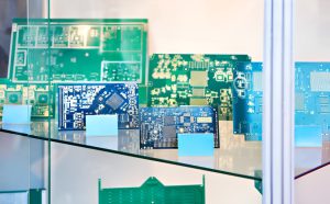
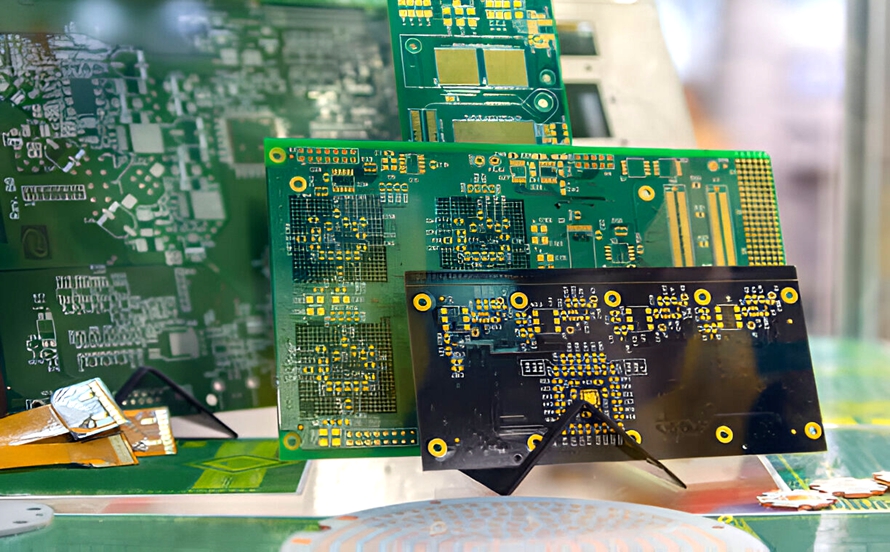
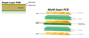
A Multilayer PCB is a printed circuit board containing multiple conductive copper layers separated by insulating dielectric materials and bonded together into a single board structure.
In conventional PCB terminology, multilayer boards generally contain four or more conductive layers, although the exact construction depends on the manufacturing technology and design requirements.
A typical multilayer PCB may include:
- Top signal layer
- Internal signal layers
- Power planes
- Ground planes
- Bottom signal layer
- Core dielectric materials
- Prepreg or other bonding dielectric materials
- Plated through-holes or other via structures
The conductive layers are interconnected using structures such as:
- Through vias
- Blind vias
- Buried vias
- Microvias in advanced HDI constructions
The number of layers can vary substantially. Four-layer and six-layer PCBs are common configurations, while more complex products can require eight, ten, twelve, sixteen, or many more layers.
The required layer count should be determined by electrical, mechanical, thermal, routing, and manufacturing requirements rather than by simply maximizing the number of layers.
Why Are Multilayer PCBs Used?
As electronic circuits become more complex, the number of interconnections between components increases. High-speed interfaces, power-distribution networks, sensors, processors, memory devices, and communication modules all require carefully planned routing.
A multilayer structure provides additional routing resources while allowing engineers to separate different electrical functions across the board.
For example, a typical stackup may allocate different layers for:
- High-speed signals
- Low-speed signals
- Power distribution
- Ground reference
- Specialized analog circuitry
- RF circuitry
This architecture provides greater flexibility than a single-sided or double-sided board.
1. Greater PCB Design Flexibility
One of the primary advantages of multilayer construction is increased PCB Design flexibility.
A single-layer board has only one conductive layer available for routing. A double-sided PCB provides additional routing space, but complex designs can still become difficult to route without excessive jumpers, long traces, or compromises in component placement.
Multilayer construction provides additional copper layers, allowing designers to distribute signals and power more efficiently.
A well-designed stackup can also provide dedicated reference planes for high-speed signals, helping create controlled and predictable return-current paths.
2. Reduced Routing Complexity
Multilayer PCBs can simplify complex routing by distributing electrical connections across multiple layers.
Instead of forcing every connection onto the top and bottom surfaces, engineers can use internal layers to route signals and distribute power.
For example:
- Outer layers can be used for component placement and selected signal routing.
- Internal layers can provide high-density signal routing.
- Dedicated power planes can distribute supply voltage.
- Ground planes can provide low-impedance return paths.
This approach can significantly reduce routing congestion and make complex circuit layouts more manageable.
However, multilayer PCBs do not automatically make a design simpler. Poor stackup planning, inadequate layer transitions, or excessive via usage can create additional signal-integrity and manufacturing problems.
3. Improved Electrical Performance
A properly designed multilayer PCB can provide better electrical performance by maintaining controlled signal paths and reference planes.
Ground and power planes can help:
- Provide continuous return-current paths
- Reduce loop area
- Improve power distribution
- Reduce electromagnetic radiation
- Support controlled impedance
- Reduce susceptibility to interference
For high-speed designs, maintaining a continuous reference plane underneath critical signal traces is especially important.
Multilayer construction therefore provides the physical architecture needed for many high-speed PCB designs.
4. Higher Functional Integration
Multilayer PCBs allow multiple electrical functions to be integrated into one compact board.
A single board may simultaneously contain:
- Processing circuits
- Memory interfaces
- Power-management circuits
- Communication interfaces
- Sensors
- Analog circuits
- Digital circuits
- RF sections
This integration can reduce the need for multiple interconnected PCB modules and simplify the overall system architecture.
5. Smaller Board Size
Increasing the number of PCB layers can allow more routing capacity within the same board area.
Instead of increasing the board’s surface area to accommodate additional circuitry, designers can add internal routing layers.
This can help achieve:
- Smaller products
- Higher component density
- Shorter interconnection paths
- Reduced connector requirements
- More compact electronic assemblies
However, adding layers does not automatically reduce manufacturing cost. More layers generally increase fabrication complexity and may increase material and processing costs.
The real benefit is the ability to achieve the required functionality within a practical form factor.
6. Higher Assembly Density
Modern electronic components increasingly use small packages and fine-pitch connections.
Multilayer PCBs provide the routing capacity required to connect these components while maintaining a compact layout.
When combined with technologies such as:
- Fine-line routing
- Microvias
- Via-in-pad
- HDI structures
- Fine-pitch BGA packages
multilayer construction can support extremely high interconnection density.
This is particularly important for smartphones, computing equipment, networking devices, medical electronics, and other compact products.
7. Fewer External Connectors
Multilayer PCBs can integrate more functions onto a single board, potentially reducing the need for separate circuit boards and external interconnections.
Internal vias provide vertical electrical connections between layers, allowing signals and power to move through the board structure.
This can help reduce:
- Connector count
- Cable length
- Interconnection space
- Mechanical complexity
Fewer external interconnections can also simplify assembly, although connector selection remains application-dependent.
8. Better Power and Ground Distribution
Dedicated power and ground layers are important advantages of many multilayer PCB stackups.
A ground plane can provide a relatively low-impedance return path, while power planes or large copper regions can distribute supply currents across the board.
Properly designed planes can help:
- Reduce voltage drop
- Improve power integrity
- Reduce return-path discontinuities
- Lower loop inductance
- Improve electromagnetic compatibility
For high-current designs, however, plane thickness, copper weight, via capacity, thermal performance, and current density must all be considered.
9. Mechanical Strength and Reliability
A multilayer PCB is constructed as a laminated composite structure. When properly designed and manufactured, the resulting board can provide good mechanical rigidity and dimensional stability.
This is particularly useful for applications that require:
- Compact mechanical packaging
- High component density
- Long-term reliability
- Resistance to vibration
- Stable dimensional performance
It is important to distinguish a conventional rigid multilayer PCB from a rigid-flex PCB. Multilayer rigid boards provide structural rigidity, while rigid-flex technology combines rigid sections with flexible circuit regions for applications requiring controlled bending.
What Are the Requirements for Multilayer PCB Design?
Successful Multilayer PCB Design requires careful planning before the layout is finalized.
1. Determine the Required Layer Count
The number of layers should be determined according to:
- Routing density
- Signal-integrity requirements
- Power-distribution requirements
- Component density
- Controlled-impedance requirements
- Thermal requirements
- Mechanical dimensions
- Manufacturing capability
A simple four-layer PCB may be sufficient for some applications, while advanced computing or communication systems may require substantially more layers.
The objective is to use an appropriate layer count rather than automatically selecting the maximum possible number of layers.
2. Develop a Balanced Stackup
Stackup design is one of the most important aspects of PCB Design.
A typical four-layer stackup might contain:
Signal / Ground / Power / Signal
More complex boards can use multiple signal and plane layers depending on the electrical architecture.
A good stackup should consider:
- Copper thickness
- Dielectric thickness
- Material Dk and Df
- Prepreg construction
- Core thickness
- Impedance requirements
- Thermal expansion
- Mechanical balance
- Manufacturing tolerances
A balanced construction can help reduce warpage and improve dimensional stability during lamination.
3. Control Dielectric Thickness
Dielectric thickness affects both mechanical construction and electrical performance.
For controlled-impedance circuits, the relationship between trace width, copper thickness, dielectric thickness, dielectric properties, and reference-plane geometry must be carefully evaluated.
For example, reducing the distance between a signal trace and its reference plane changes the electromagnetic field distribution and therefore affects characteristic impedance.
This is why the final stackup should be developed in cooperation with the PCB manufacturer rather than relying solely on nominal material thicknesses.
4. Plan Power and Ground Layers
Power and ground layers should be assigned according to the electrical architecture of the product.
A continuous ground plane can provide a reliable return path for high-speed signals.
Designers should avoid unnecessary reference-plane splits beneath critical high-speed traces because return current may be forced to take a longer path, increasing loop area and potentially degrading signal integrity and EMI performance.
5. Optimize Via Structures
Vias are essential for connecting different layers, but every via also consumes routing space and introduces electrical parasitics.
Designers may use:
- Through vias
- Blind vias
- Buried vias
- Microvias
- Stacked microvias
- Staggered microvias
The appropriate structure depends on the board’s stackup and density requirements.
For high-speed designs, long via stubs can create unwanted capacitance, inductance, and resonant behavior. Backdrilling or other via-transition strategies may therefore be considered when appropriate.
6. Consider Signal Integrity
As data rates increase, multilayer PCB designs require careful signal-integrity analysis.
Important considerations include:
- Controlled impedance
- Trace length
- Differential-pair routing
- Return-current paths
- Crosstalk
- Via transitions
- Reference-plane continuity
- Power integrity
- Connector transitions
Signal integrity should be considered during stackup planning rather than treated as a final-stage correction.
7. Design for Manufacturing
A multilayer PCB must be designed according to realistic manufacturing capabilities.
DFM review should evaluate:
- Minimum trace width
- Minimum spacing
- Hole diameter
- Annular ring
- Copper-to-edge clearance
- Layer registration
- Via structure
- Aspect ratio
- Solder-mask clearance
- Copper balancing
- Board thickness tolerance
- Panelization
The manufacturer’s actual process capability should be used when defining these values.
Multilayer PCB Manufacturing Process
The PCB Manufacturing process for multilayer boards is more complex than that of single-sided or double-sided PCBs.
A simplified process can include the following stages.
1. Inner-Layer Circuit Formation
The copper layers of the inner cores are processed using imaging, development, etching, stripping, and inspection.
The required internal signal, power, and ground patterns are formed during this stage.
2. Inner-Layer Inspection
After inner-layer etching, AOI is commonly used to identify pattern defects before the layers are laminated.
Potential defects include:
- Open circuits
- Shorts
- Missing copper
- Excess copper
- Pattern deviations
Detecting defects before lamination is important because an inner-layer defect becomes much more difficult to access after the board has been assembled.
3. Layup and Lamination
The processed cores, prepreg materials, and copper foils are carefully arranged according to the approved stackup.
The multilayer assembly is then laminated using controlled temperature and pressure.
During lamination:
- Resin flows into the required spaces.
- Dielectric materials bond the layers together.
- Heat cures the resin.
- Pressure consolidates the stack.
- Layer registration is maintained.
The exact lamination profile depends on the laminate system, resin content, copper distribution, board thickness, and equipment.
4. Drilling
After lamination, holes are drilled to create the required interconnections.
Depending on the design, these may include:
- Plated through-holes
- Mechanical blind vias
- Other specialized via structures
Advanced HDI multilayer boards may undergo additional laser-drilling operations during sequential build-up cycles.
5. Desmear and Hole Preparation
Mechanical drilling can leave resin smear inside the drilled holes.
A desmear and hole-conditioning process may therefore be used to prepare the hole walls for reliable metallization.
Proper hole preparation is important for achieving reliable plated-through-hole connections.
6. Electroless Copper and Electroplating
A conductive copper seed layer is established on the hole walls, after which electroplating can increase copper thickness.
This process creates reliable electrical connections between the required PCB layers.
For advanced HDI structures, additional copper-plating and microvia-filling processes may be required.
7. Outer-Layer Circuit Formation
The outer copper layers are patterned and processed according to the PCB design.
The manufacturing sequence may include:
- Lamination or resist application
- Imaging
- Development
- Copper plating
- Tin or other etch-resist processes
- Etching
- Resist stripping
- Inspection
Process parameters must be carefully controlled to maintain the required trace geometry.
8. Solder Mask Application
After the copper circuitry is completed, solder mask is applied to protect the board surface and prevent unintended solder bridging.
The process generally includes:
- Surface preparation
- Solder-mask coating
- Imaging
- Development
- Curing
- Inspection
The solder mask also provides electrical insulation between exposed conductive areas where required.
9. Surface Finish
The exposed copper pads are treated with an appropriate surface finish to improve solderability and protect the copper from oxidation.
Common options include:
- ENIG
- ENEPIG
- HASL
- Lead-free HASL
- OSP
- Immersion tin
- Immersion silver
The correct surface finish depends on component pitch, assembly process, reliability requirements, storage conditions, and application environment.
10. Electrical Testing
Electrical testing verifies the connectivity and isolation of the finished multilayer PCB.
Common methods include:
- Flying-probe testing
- Fixture-based testing
- Continuity testing
- Isolation testing
Additional testing may be performed for high-speed or high-reliability applications.
For controlled-impedance boards, impedance testing and test coupons may be used to verify that critical transmission-line structures meet the specified requirements.
Multilayer PCB Applications
The flexibility of multilayer construction makes it suitable for a wide range of applications.
Consumer Electronics
Multilayer PCBs are widely used in:
- Smartphones
- Laptops
- Tablets
- Wearable devices
- Digital cameras
- Home electronics
Compact dimensions and high component density make multilayer construction particularly useful in modern consumer products.
Telecommunications
Networking and communication equipment often require multiple high-speed signal layers, power planes, and carefully controlled reference structures.
Applications include:
- Network switches
- Routers
- Wireless communication equipment
- Base-station electronics
- Optical communication equipment
Automotive Electronics
Modern vehicles contain numerous electronic control systems.
Multilayer PCBs can be used in:
- Engine control electronics
- ADAS systems
- Infotainment
- Body-control modules
- Automotive networking
- Battery-management systems
- Power electronics
Medical Devices
Medical equipment often requires reliable, compact, and electrically sophisticated circuit assemblies.
Multilayer PCBs may be used in:
- Patient monitoring equipment
- Diagnostic instruments
- Imaging systems
- Laboratory equipment
- Portable medical devices
Industrial Electronics
Industrial automation and control systems can use multilayer PCBs for:
- PLC systems
- Motor controllers
- Industrial computers
- Power-management equipment
- Measurement systems
- IoT gateways
Aerospace and Defense Electronics
Where high integration and controlled electrical performance are required, multilayer PCB technology can be used in sophisticated aerospace and defense electronic systems.
These applications may require additional material, reliability, inspection, and qualification requirements depending on the product.
Multilayer PCB vs. Single-Layer PCB
The primary difference is the number of conductive layers and the resulting routing capacity.
| Feature | Single-Layer PCB | Multilayer PCB |
|---|---|---|
| Conductive layers | One | Multiple |
| Routing density | Limited | High |
| Circuit complexity | Low to moderate | Moderate to very high |
| Power/ground planes | Limited | Dedicated planes can be incorporated |
| High-speed design | More constrained | Greater stackup flexibility |
| Component density | Lower | Higher |
| Manufacturing complexity | Lower | Higher |
| Typical cost | Lower | Higher |
| Typical applications | Simple electronics | Complex electronic systems |
Multilayer construction is not automatically better for every product. A simple circuit may not justify the additional manufacturing complexity of a multilayer board. The appropriate PCB structure should be determined by the actual electrical and mechanical requirements.
Key Challenges in Multilayer PCB Manufacturing
Although multilayer technology provides substantial design flexibility, it also introduces additional manufacturing challenges.
Layer Registration
All layers must remain accurately aligned during lamination and drilling.
Warpage
Uneven copper distribution and unbalanced construction can contribute to board warpage.
Dielectric Thickness Control
Variations in dielectric thickness can affect both board thickness and controlled-impedance performance.
Via Reliability
Plated-through holes and other via structures must withstand thermal and mechanical stresses throughout the product’s service life.
Signal Integrity
High-speed designs require appropriate reference planes, controlled impedance, and carefully managed via transitions.
Manufacturing Cost
Additional layers, materials, drilling, plating, lamination, inspection, and testing can increase production costs.
For this reason, multilayer PCB design should always balance performance requirements against manufacturing complexity.
Multilayer PCB Manufacturing with Kingda
A successful multilayer PCB requires close coordination between engineering design and manufacturing.
Kingda can support multilayer PCB projects involving:
- Multilayer PCB fabrication
- High-density routing
- Controlled-impedance PCB
- HDI structures
- Fine-line circuitry
- Blind and buried vias
- High-current copper designs
- Surface finishes
- AOI and electrical testing
- DFM engineering review
During the early engineering stage, the PCB design can be evaluated together with the proposed stackup, material system, copper thickness, via structure, and manufacturing tolerances.
This approach helps identify potential production risks before fabrication and can reduce unnecessary design iterations.
Conclusion
The development of Multilayer PCB technology has fundamentally expanded what engineers can achieve with printed circuit boards. By combining multiple copper layers with dielectric materials and reliable interlayer connections, multilayer construction provides greater routing density, improved power and ground distribution, better signal-integrity control, and higher functional integration.
A successful multilayer board begins with a carefully developed PCB Design. Layer count, stackup, dielectric thickness, copper weight, power and ground planes, via structures, impedance requirements, thermal performance, and DFM considerations must be evaluated together.
The subsequent PCB Manufacturing process also requires precise control of inner-layer fabrication, lamination, drilling, plating, outer-layer processing, solder-mask application, surface finishing, and electrical testing.
As electronic products continue to become smaller and more complex, multilayer PCB technology will remain an important foundation for high-density and high-performance electronic systems. Choosing the appropriate layer structure and manufacturing process allows engineers to achieve the required functionality while maintaining reliability, manufacturability, and cost control.