What Is a Printed Circuit Board? PCB Design, PCB Manufacturing, Assembly & Benefits
Electronic devices are complex systems that combine a printed circuit board with a mechanical enclosure and a wide range of electronic components. At the center of this system is the printed circuit board (PCB), which provides both the physical platform for component mounting and the electrical connections required for the device to operate.
A well-designed PCB is essential to the functionality, reliability, and manufacturability of modern electronics. Without a PCB or another suitable interconnection technology, electronic devices would require complicated point-to-point wiring, making them larger, less reliable, and more difficult to manufacture and service.
Components such as resistors, capacitors, inductors, microcontrollers, connectors, LEDs, sensors, and integrated circuits can be securely mounted on a PCB and electrically interconnected through copper traces, vias, and other conductive structures.
The evolution from traditional wired electronics to modern PCB-based systems has transformed the electronics industry. Earlier electronic products were often large, difficult to operate, and challenging to repair because of complicated wiring and bulky components. Modern electronics, by contrast, are smaller, more capable, easier to operate, and increasingly reliable.
Advances in PCB Design, PCB Manufacturing, PCB Assembly, PCB testing, and miniature component packaging have made it possible to build compact electronic products with sophisticated functionality, high processing capabilities, and multiple integrated functions.
What Is a Printed Circuit Board?
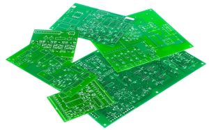
A printed circuit board is an engineered interconnection structure consisting of conductive copper layers, dielectric insulating materials, and mechanical features that allow electronic components to be mounted and electrically connected.
A typical PCB may contain copper traces, pads, vias, solder mask, silkscreen, and one or more dielectric layers. In multilayer boards, multiple copper layers are interconnected through plated through-holes, blind vias, buried vias, or microvias, depending on the design requirements.
Instead of using large bundles of individual wires, a PCB uses precisely manufactured copper traces to establish electrical connections between components. This approach makes circuits more compact, repeatable, and suitable for automated manufacturing.
During PCB Design, engineers define the component placement, trace routing, layer stackup, power distribution, grounding structure, impedance requirements, and manufacturing constraints. Appropriate spacing between conductive features is also required to reduce the risk of electrical shorts, unwanted coupling, and other signal-integrity problems.
PCBs are used in almost every category of modern electronics, including smartphones, televisions, laptops, keyboards, tablets, automotive electronics, LED lighting, LED drivers, industrial equipment, medical devices, telecommunications equipment, and consumer appliances.
Common PCB types include:
- Single-Sided PCB – contains conductive circuitry primarily on one side of the substrate.
- Double-Sided PCB – uses copper circuitry on both sides and typically relies on plated holes for interconnection.
- Multilayer PCB – contains multiple copper layers separated by dielectric materials for higher routing density and more complex circuits.
- Rigid PCB – uses a rigid substrate, commonly FR-4, to provide mechanical support.
- Flexible PCB – uses a flexible substrate such as polyimide for applications requiring bending or dynamic movement.
- Rigid-Flex PCB – combines rigid and flexible sections within one interconnected PCB structure.
This variety allows PCB technology to support applications ranging from simple consumer electronics to high-speed computing, automotive systems, medical equipment, aerospace electronics, and industrial control systems.
Advantages of Using Printed Circuit Boards
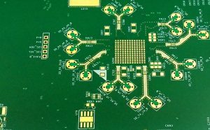
PCBs provide numerous benefits throughout electronic product design, manufacturing, assembly, testing, and maintenance. The following are some of the most important advantages.
1. Smaller and More Compact Electronic Devices
One of the most important benefits of PCB technology is electronic miniaturization.
Traditional point-to-point wiring requires individual wires and connections between components. These wires occupy significant space and can introduce problems such as loose connections, complicated assembly, and difficult troubleshooting.
A PCB replaces much of this physical wiring with precisely patterned copper traces. Components can therefore be arranged in a highly organized and compact structure.
Modern PCB Assembly processes also support increasingly small surface-mount components. SMD components can be mounted directly onto PCB pads, allowing engineers to achieve considerably higher component density than many traditional through-hole designs.
By combining advanced PCB layout techniques with miniature components, engineers can develop compact circuit boards while integrating more functions into a smaller physical area.
This is particularly important for smartphones, wearable devices, IoT products, portable medical equipment, automotive electronics, and other space-constrained applications.
2. Lower Manufacturing Costs
Modern PCB Manufacturing relies heavily on automation, computer-controlled equipment, precision imaging, automated optical inspection, and highly repeatable production processes.
These technologies can improve manufacturing consistency while reducing manual operations and the probability of human assembly errors.
PCBs are also highly suitable for mass production. Once the design and manufacturing process have been validated, manufacturers can produce large quantities of boards using standardized production processes.
Panelization is another important manufacturing strategy. Multiple PCB units can be arranged on a larger production panel, allowing manufacturing processes to handle several boards simultaneously. This can improve material utilization, reduce handling time, and lower the manufacturing cost per board when the design and production volume are suitable.
However, PCB cost depends on many factors, including:
- Number of PCB layers
- Board dimensions
- Copper thickness
- Material selection
- Minimum trace width and spacing
- Via structure
- Surface finish
- Component density
- Manufacturing volume
- Testing requirements
- PCB Assembly complexity
Therefore, cost optimization should begin during the design stage rather than after the PCB has already been manufactured.
3. PCBs Enable Electronic Innovation
Innovation in electronics often begins with an engineering concept, followed by circuit design, prototyping, testing, and optimization. PCB technology provides the physical platform required to turn these concepts into functional electronic prototypes.
Engineers can develop a PCB prototype to evaluate circuit behavior, component placement, signal performance, thermal characteristics, and mechanical integration before moving to large-scale production.
Modern technologies such as artificial intelligence, machine learning, 5G communications, high-speed computing, Internet of Things devices, robotics, and industrial automation all depend on increasingly sophisticated electronic hardware.
These applications often require PCBs with:
- High routing density
- Controlled impedance
- High-speed signal transmission
- Efficient power distribution
- Reliable grounding
- Effective thermal management
- Electromagnetic compatibility
- Advanced component packaging
As a result, PCB technology continues to evolve alongside electronic innovation.
For example, high-performance computing and AI hardware can require advanced multilayer or HDI structures to accommodate dense interconnections and demanding power and signal requirements. Similarly, automotive electronics and industrial automation systems increasingly require reliable PCBs capable of operating under demanding environmental conditions.
4. Reduced Electrical Noise and Improved Signal Integrity
PCB design has a direct influence on electrical noise, signal integrity, and electromagnetic compatibility.
A poorly designed board can experience excessive crosstalk, ground bounce, electromagnetic interference, voltage fluctuations, or signal reflections. These problems can negatively affect the reliability and performance of electronic equipment.
A carefully engineered PCB can reduce these risks through appropriate:
- Component placement
- Trace routing
- Grounding strategies
- Power distribution
- Layer stackup
- Reference planes
- Differential-pair routing
- Decoupling capacitor placement
- Via design
- Electromagnetic shielding
For high-speed applications, PCB Design must also consider transmission-line effects, controlled impedance, return-current paths, dielectric properties, copper geometry, and via structures.
A continuous reference plane and a well-designed return path are particularly important for maintaining signal integrity.
Therefore, PCB layout is not simply about connecting components. It is an essential part of the electrical engineering process.
5. Easier Testing, Troubleshooting, and Repair
Compared with complex point-to-point wiring systems, a well-designed PCB can make electronic troubleshooting and maintenance more systematic.
Modern boards can be designed according to Design for Manufacturability (DFM), Design for Assembly (DFA), and Design for Testability (DFT) principles.
Reference designators, component markings, test points, and clearly organized layouts help engineers identify and inspect components during testing and maintenance.
Test points can provide convenient access for measuring:
- Voltage
- Current
- Clock signals
- Digital signals
- Analog signals
- Power-rail conditions
Engineers can also use schematics, PCB layout files, and layer information to trace electrical connections and identify potential faults.
For repair operations, defective components can often be removed and replaced using appropriate soldering or rework equipment. The exact repair method depends on the component package, PCB construction, thermal characteristics, and board reliability requirements.
In production environments, automated inspection and electrical testing can further improve fault detection. Common technologies include AOI, ICT, flying-probe testing, and functional testing.
6. Supports High-Density Component Integration
Another major advantage of PCB technology is its ability to support high-density electronic assemblies.
Modern SMD packages, fine-pitch components, BGAs, microcontrollers, sensors, memory devices, and other advanced packages can be integrated onto compact PCB layouts.
High-density interconnect technologies such as HDI can further increase routing capability through structures such as microvias and sequentially laminated build-up layers.
This allows engineers to integrate more electronic functions without proportionally increasing the physical size of the product.
High-density PCB technology is particularly valuable in:
- Smartphones and tablets
- Wearable electronics
- Medical devices
- Automotive electronics
- Networking equipment
- High-performance computing
- Industrial control systems
- Aerospace electronics
7. Reliable and Repeatable Electrical Connections
PCB manufacturing creates standardized conductive paths between components. Unlike manually assembled wire harnesses, these connections are defined directly by the PCB layout and reproduced through controlled manufacturing processes.
This repeatability is particularly important for mass production.
The reliability of a PCB depends on factors such as material selection, copper quality, plating, solder joints, thermal cycling, mechanical stress, environmental conditions, and manufacturing process control.
A properly designed and manufactured PCB can provide stable electrical connections throughout the intended service life of an electronic product.
How PCB Design Affects Electronic Product Performance
The PCB is not simply a passive platform for mounting components. Its design directly influences the electrical, mechanical, thermal, and manufacturing characteristics of the final product.
During PCB Design, engineers need to consider several interconnected factors.
Electrical Design
Electrical design determines how power and signals travel through the board. Engineers must consider trace width, spacing, impedance, current capacity, grounding, return paths, and signal integrity.
Thermal Design
High-power components can generate significant heat. PCB designers may need to use larger copper areas, thermal vias, heat-spreading structures, metal-core materials, or other thermal-management techniques.
Mechanical Design
The PCB must fit inside the product enclosure and align correctly with connectors, switches, displays, mounting holes, heat sinks, and other mechanical structures.
Manufacturing Design
A theoretically functional design may still be difficult or expensive to manufacture. DFM rules should therefore be considered early, including minimum trace and spacing requirements, hole sizes, solder mask clearance, component spacing, panelization, and fabrication tolerances.
PCB Manufacturing Process
A typical PCB manufacturing process includes multiple controlled stages.
1. Inner-Layer Fabrication
For multilayer PCBs, inner copper layers are imaged, etched, inspected, and prepared for lamination.
2. Layup and Lamination
Copper foils, cores, and prepreg materials are arranged according to the specified stackup. Heat and pressure are then applied to create a consolidated multilayer structure.
3. Drilling
Mechanical drilling or laser drilling creates the required holes and vias. The drilling technology depends on the PCB structure and design requirements.
4. Hole Preparation and Copper Plating
After drilling, hole walls may undergo desmear and other preparation processes. Electroless copper and subsequent electroplating establish conductive connections through plated holes and across relevant copper surfaces.
5. Outer-Layer Circuit Formation
The outer copper layers are patterned through imaging, plating, etching, and related processes to form the required circuitry.
6. Solder Mask Application
A solder mask is applied to protect exposed copper areas and reduce the risk of unintended solder bridging during assembly. Openings are created over pads and other areas that must remain solderable or electrically accessible.
7. Surface Finish
Depending on the application, the PCB may use HASL, ENIG, OSP, immersion tin, immersion silver, ENEPIG, or another suitable surface finish.
8. PCB Testing and Inspection
Manufacturers may perform AOI, electrical testing, dimensional inspection, solder mask inspection, surface-finish inspection, and other quality-control procedures.
The exact process varies according to PCB type, material, layer count, technology, and customer requirements.
Common Applications of Printed Circuit Boards
PCBs are used throughout virtually every major electronics sector.
Consumer Electronics
Smartphones, laptops, televisions, tablets, gaming devices, smart home products, and wearable electronics all rely heavily on PCBs.
Automotive Electronics
Modern vehicles contain numerous electronic control units and systems for power management, infotainment, lighting, sensing, safety, communication, and vehicle control.
Medical Electronics
Medical equipment requires reliable and carefully controlled electronic assemblies. PCBs can be found in monitoring equipment, diagnostic systems, imaging equipment, portable medical devices, and laboratory instruments.
Telecommunications
Routers, switches, wireless communication equipment, base stations, optical communication systems, and networking hardware use advanced PCBs to support high-speed data transmission.
Industrial Equipment
Industrial automation, motor controllers, power supplies, robotics, measurement equipment, and control systems depend on PCBs for reliable electronic control and communication.
Aerospace and Defense Electronics
Aerospace applications can require PCBs with stringent reliability, environmental, mechanical, and electrical performance requirements.
PCB vs. Traditional Wiring
The development of PCB technology has largely replaced complicated point-to-point wiring in many modern electronic products.
| Feature | PCB-Based Electronics | Traditional Point-to-Point Wiring |
|---|---|---|
| Size | Compact and highly organized | Often larger |
| Connection method | Copper traces and vias | Individual wires |
| Manufacturing | Highly automatable | More labor-intensive |
| Repeatability | High | Depends more heavily on assembly |
| Component density | High | Generally lower |
| Troubleshooting | Structured through schematics and test points | Can be more difficult in complex wiring |
| Mass production | Well suited | Less efficient for many compact products |
| Design flexibility | High | More limited as complexity increases |
The appropriate interconnection method still depends on the product, electrical requirements, mechanical structure, production volume, and cost targets.
Choosing the Right PCB Manufacturing Partner
Selecting a capable PCB manufacturing partner is an important part of developing reliable electronic products.
A suitable manufacturer should be able to support the technical requirements of the project throughout fabrication, assembly, testing, and quality control.
When evaluating a PCB supplier such as Kingda, engineers and purchasing teams should consider:
- PCB manufacturing capabilities
- Layer-count range
- Material options
- Copper thickness capability
- Minimum trace and spacing capability
- Via and HDI technology
- Surface-finish options
- PCB assembly capabilities
- AOI and electrical testing
- DFM support
- Quality-management systems
- Production capacity
- Prototype and mass-production support
- Engineering communication and technical support
Early communication between the PCB designer and manufacturer can help identify manufacturability problems before production begins and reduce unnecessary redesigns.
Conclusion
A printed circuit board is one of the fundamental technologies behind modern electronic products. By replacing complicated wiring with precisely engineered copper interconnections, PCBs enable electronic devices to become smaller, more reliable, more functional, and easier to manufacture.
The advantages of PCB technology include compact product design, high component density, automated manufacturing, repeatable electrical connections, improved signal integrity, easier testing and maintenance, and support for advanced electronic innovation.
As technologies such as AI, 5G, IoT, automotive electronics, robotics, medical equipment, and high-performance computing continue to evolve, the requirements placed on PCB Design and PCB Manufacturing will also become increasingly demanding.
For engineers and electronics manufacturers, understanding PCB structure, design principles, manufacturing processes, assembly requirements, and testing methods is essential for developing reliable and commercially viable electronic products.
SEO Keywords
PCB Design, PCB Manufacturing, Printed Circuit Board, PCB Assembly, PCB Manufacturing Process, Multilayer PCB, PCB Testing, HDI PCB, PCB Design Services, PCB Assembly Services
Google TDK
SEO Title:
What Is a Printed Circuit Board? PCB Design, PCB Manufacturing & Assembly
Meta Description:
Learn what a printed circuit board is, how PCB Design and PCB Manufacturing work, and why PCB Assembly, testing, miniaturization, and signal integrity are essential to modern electronics.
Meta Keywords:
PCB Design, PCB Manufacturing, Printed Circuit Board, PCB Assembly, PCB Manufacturing Process, Multilayer PCB, PCB Testing, HDI PCB