PCB Trace Materials: PCB Design, PCB Manufacturing & Copper Trace Guide
Electronic devices have transformed almost every aspect of modern life. From smartphones and computers to automotive systems, medical equipment, industrial controllers, and communication devices, these products rely on sophisticated electronic circuits to perform their intended functions.
At the center of many electronic systems is the printed circuit board (PCB). A PCB provides the physical foundation for electronic components while also creating the electrical pathways that allow those components to communicate with one another.
The internal structure of a PCB is more sophisticated than it may appear. A circuit board is not made from a single material. Instead, it consists of conductive layers, dielectric materials, solder mask, surface finishes, and other materials that work together as an integrated structure.
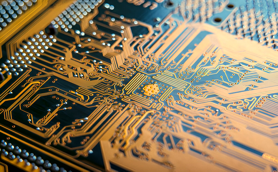
If you examine a multilayer PCB from the side, you can see alternating conductive and insulating layers interconnected by vertical structures such as plated through-holes, blind vias, buried vias, or microvias. From the top, a PCB may appear as a flat board covered with thin conductive lines known as PCB traces.
These traces form the electrical pathways between components. Their material, geometry, thickness, width, spacing, and surface condition can significantly affect the electrical and mechanical performance of the finished board.
Among all available conductive materials, copper remains the dominant material for PCB traces because it provides an excellent combination of electrical conductivity, thermal performance, manufacturability, availability, and cost.
This article explains what PCB traces are, why copper is widely used as a PCB trace material, the key principles of trace design, common trace defects, and important considerations during PCB Manufacturing.
What Is a PCB Trace?
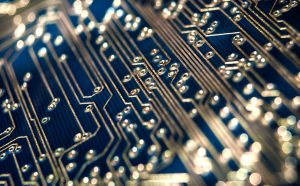
A PCB trace is a patterned strip of conductive material, normally copper, that carries electrical signals or power between components, pads, vias, and other conductive structures on a printed circuit board.
PCB traces function much like pathways within an electrical system. They provide controlled routes through which current and electrical signals can travel between different parts of the circuit.
In a simple single-sided PCB, traces are primarily formed on one side of the board. In a double-sided PCB, traces can be routed on both outer layers and interconnected through plated holes. In a multilayer PCB, traces can exist on multiple internal and external copper layers.
During PCB Design, engineers determine where traces should be placed and how they should connect different components. Important parameters include:
- Trace width
- Trace thickness
- Trace length
- Trace spacing
- Copper weight
- Layer position
- Impedance requirements
- Current capacity
- Thermal conditions
- Manufacturing tolerances
- Signal frequency and edge rate
Copper traces are normally separated from one another by dielectric material or solder mask, depending on their location and structure. Proper spacing helps reduce the risk of unintended electrical connections and excessive capacitive or inductive coupling.
For high-speed circuits, a PCB trace can also form part of a transmission-line structure. For example, a surface trace referenced to a nearby ground plane can function as a microstrip, while an internal trace between reference planes can form a stripline.
Therefore, PCB traces are not simply pieces of metal. Their geometry and surrounding dielectric environment can directly influence impedance, signal integrity, electromagnetic compatibility, and power-delivery performance.
Why Is Copper the Most Common PCB Trace Material?

Copper is the most widely used PCB trace material because it offers a highly practical balance of electrical, thermal, mechanical, and economic properties.
Although other conductive materials can be used for specialized PCB technologies, copper is the standard choice for most conventional printed circuit boards.
Excellent Electrical Conductivity
Copper has high electrical conductivity, allowing current and signals to travel efficiently through relatively thin conductive paths.
This property is particularly important for PCB traces because excessive electrical resistance can result in voltage drop, power dissipation, and localized heating.
Copper’s conductivity is significantly higher than that of materials such as aluminum and steel, making it well suited to PCB interconnection applications.
The actual electrical performance of a PCB trace, however, depends not only on the material but also on trace width, thickness, length, temperature, surface roughness, and operating frequency.
Good Availability and Cost Efficiency
Copper is considerably more economical than highly conductive precious metals such as gold and silver.
Gold, for example, is commonly used as part of certain PCB surface finishes because of its chemical stability and solderability characteristics, but using solid gold as the primary bulk material for conventional PCB traces would be economically impractical.
Copper provides the conductivity required for PCB circuitry while remaining suitable for large-scale commercial manufacturing.
This combination of performance and cost is one of the main reasons copper has become the industry standard for PCB conductive layers.
High Thermal Conductivity
Copper also provides excellent thermal conductivity.
Its ability to spread heat makes copper useful not only for carrying current but also for distributing heat across PCB structures.
Large copper pours, planes, thermal pads, and copper-filled vias can be incorporated into a PCB design to help transfer heat away from power devices and other heat-generating components.
It is important to distinguish thermal conductivity from overall PCB thermal performance. The final temperature of a PCB depends on many factors, including copper area, board thickness, airflow, component power dissipation, thermal vias, substrate material, enclosure design, and cooling conditions.
Basic PCB Trace Design Guidelines
During PCB Design, engineers must balance electrical performance, thermal requirements, available board area, and manufacturing capability.
The following considerations are especially important when designing copper traces.
1. Controlled Impedance
For high-speed and RF circuits, trace geometry plays an important role in determining characteristic impedance.
Trace width, copper thickness, dielectric thickness, dielectric constant, trace-to-plane spacing, differential spacing, and surrounding structures all influence impedance.
A wider trace does not automatically mean better impedance control. Instead, the trace geometry must be calculated against the selected PCB stackup and target impedance.
For example, a 50-ohm single-ended transmission line or a 90-ohm or 100-ohm differential pair requires a specific combination of trace geometry and dielectric structure.
Engineers should therefore define the PCB stackup before finalizing critical high-speed routing.
Trace Neck-Down
A trace neck-down is a deliberate reduction in trace width used when a signal must pass through a restricted area, such as between component pads or through a high-density routing region.
However, changing trace geometry can introduce an impedance discontinuity.
For high-speed signals, unnecessary neck-down sections should therefore be minimized. If a transition is unavoidable, engineers should evaluate its electrical impact and maintain consistent geometry wherever practical.
2. Current-Carrying Capacity
Trace width and copper thickness directly affect the current-carrying capability of a PCB trace.
A trace with greater cross-sectional area generally has lower DC resistance and can carry more current for a given allowable temperature rise.
The current capacity of a PCB trace depends on several factors, including:
- Copper thickness
- Trace width
- Trace length
- Allowable temperature rise
- Internal or external layer location
- Ambient temperature
- Thermal environment
- Nearby copper structures
For high-current circuits, engineers may use wider traces, heavier copper, copper pours, planes, or multiple parallel paths.
Industry guidelines such as IPC recommendations can provide useful starting points for determining trace width based on current and allowable temperature rise. Final dimensions should still be validated against the actual design and manufacturing requirements.
3. Thermal Distribution
As electronic products become smaller while their processing and power requirements increase, current density and component power density can rise significantly.
This creates additional thermal-management challenges.
PCB designers should consider trace width, copper thickness, copper area, current, component placement, thermal vias, and heat-spreading structures when designing power circuits.
Heat-sensitive components should also be positioned appropriately relative to high-power devices and other heat sources.
For multilayer PCBs, internal copper planes can provide additional thermal spreading and current distribution.
However, copper alone cannot solve every thermal problem. The overall thermal design must also consider the enclosure, airflow, heat sinks, interface materials, component package, and operating environment.
4. Trace Resistance
Copper is an excellent conductor, but it is not a zero-resistance material.
The resistance of a PCB trace is primarily related to copper resistivity, trace length, and cross-sectional area.
A simplified relationship is:
R = ρL/A
where:
- R is resistance
- ρ is the resistivity of the conductor
- L is trace length
- A is cross-sectional area
Increasing trace width or copper thickness increases the cross-sectional area and therefore generally reduces resistance.
Longer traces, on the other hand, increase resistance.
This becomes particularly important in power-distribution networks, high-current circuits, precision analog systems, and applications where voltage drop must be tightly controlled.
5. PCB Manufacturing and Assembly Considerations
A theoretically ideal trace layout may not always be practical to manufacture.
Before finalizing the design, engineers should communicate with the PCB manufacturer regarding fabrication capabilities and tolerances.
Important parameters may include:
- Minimum trace width
- Minimum spacing
- Copper thickness
- Etching capability
- Registration tolerance
- Via dimensions
- Solder mask clearance
- Surface-finish requirements
- Impedance-control capability
The selected surface finish can also affect exposed copper pads and solderable surfaces.
Common PCB surface finishes include:
- HASL
- Lead-free HASL
- OSP
- ENIG
- Immersion tin
- Immersion silver
- ENEPIG
The appropriate finish depends on the component package, soldering process, environmental requirements, shelf life, electrical requirements, and cost considerations.
Common PCB Trace Defects
PCB traces can develop defects during fabrication, assembly, handling, or operation. Such defects can affect electrical continuity, signal integrity, reliability, and product functionality.
Understanding common trace defects is therefore an important part of PCB Manufacturing quality control.
1. PCB Trace Short Circuit
A short circuit occurs when two conductive features that should remain electrically isolated become unintentionally connected.
A short may result from:
- Excessive copper remaining after etching
- Insufficient spacing
- Trace over-etching or under-etching
- Manufacturing contamination
- Solder bridging
- Design errors
- Conductive debris
In high-density PCBs, even a small fabrication deviation can create an unintended connection between adjacent traces or pads.
Automated optical inspection, electrical testing, and appropriate design-rule checking can help detect and prevent these problems.
2. PCB Trace Open Circuit
An open circuit occurs when an intended conductive path is interrupted.
An open trace may be caused by:
- Excessive etching
- Scratches
- Copper peeling
- Mechanical damage
- Plating defects
- Cracks
- Manufacturing contamination
- Insufficient copper formation
An open circuit prevents current or signals from reaching the intended destination and can cause complete or partial circuit failure.
Electrical continuity testing is commonly used to identify open circuits after fabrication.
3. Missing PCB Trace
A missing trace occurs when a required conductive path is absent from the manufactured board.
This problem may result from:
- Incorrect PCB design data
- Artwork or imaging errors
- Manufacturing process problems
- Excessive etching
- Data-conversion errors
- Fabrication defects
Because a missing trace can completely interrupt an electrical connection, manufacturers use inspection and electrical testing processes to verify the finished PCB.
How to Prevent PCB Trace Problems
Many PCB trace problems can be reduced through a combination of good design practices, DFM review, controlled manufacturing processes, and electrical testing.
Use Appropriate Trace Width and Spacing
Trace width and spacing should be selected according to electrical requirements and the manufacturer’s actual fabrication capability.
Designing traces significantly below the manufacturer’s reliable process capability can increase fabrication difficulty and reduce manufacturing margins.
Avoid Unnecessary Long, Narrow Traces
Long, narrow traces can increase resistance and voltage drop, particularly in power circuits.
Where appropriate, designers should use wider traces, copper pours, planes, or parallel routing structures.
Maintain Consistent High-Speed Trace Geometry
For controlled-impedance circuits, unnecessary changes in trace width, spacing, reference-plane distance, or routing structure should be minimized.
Differential pairs should be routed with appropriate spacing and consistent geometry while maintaining a suitable reference plane and return path.
Perform DFM Checks Before Manufacturing
Design for Manufacturability (DFM) analysis helps identify potential fabrication problems before the design enters production.
Typical DFM checks include:
- Trace width and spacing
- Copper-to-edge clearance
- Hole sizes
- Annular rings
- Solder mask openings
- Component spacing
- Via structures
- Layer registration
- Manufacturing tolerances
Early DFM review can reduce redesigns, production delays, and unnecessary manufacturing costs.
Perform PCB Inspection and Electrical Testing
A comprehensive PCB Testing strategy can identify both visible and electrical defects.
Depending on the product and production volume, manufacturers may use:
- AOI
- Electrical continuity testing
- Flying-probe testing
- ICT
- Functional testing
- X-ray inspection for suitable assemblies
The appropriate testing method depends on PCB complexity, production volume, component technology, and reliability requirements.
How Kingda Supports PCB Trace Manufacturing
For electronics companies developing new products, PCB trace performance depends on both the quality of the design and the manufacturer’s ability to reproduce the specified geometry consistently.
Kingda can support customers throughout the PCB development process, from prototype fabrication to production manufacturing and assembly.
Engineering teams can evaluate important requirements such as PCB material, copper thickness, trace width and spacing, controlled impedance, surface finish, layer stackup, via structures, and testing requirements before production.
By considering manufacturability during the design stage, engineers can develop PCB layouts that balance electrical performance, thermal requirements, manufacturing capability, reliability, and cost.
Conclusion
PCB traces are fundamental conductive structures that allow components and circuits to communicate and distribute electrical power. Although PCB technology involves many different materials, copper remains the dominant PCB trace material because of its excellent electrical conductivity, thermal performance, availability, and cost efficiency.
Successful trace design requires more than simply connecting two components. Engineers must consider impedance, current-carrying capacity, thermal distribution, resistance, trace geometry, manufacturing tolerances, and signal integrity.
At the same time, defects such as short circuits, open circuits, missing traces, scratches, and plating problems can compromise PCB reliability. Careful PCB Design, DFM analysis, controlled PCB Manufacturing, inspection, and electrical testing are therefore essential.
As electronic products continue to become smaller, faster, and more powerful, PCB trace technology will become increasingly important. Selecting appropriate materials and designing traces according to electrical and manufacturing requirements can help engineers create reliable, manufacturable, and high-performance electronic products.