Bare PCB: PCB Design, PCB Manufacturing, Types, Materials & Applications
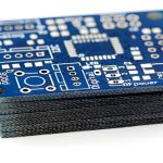
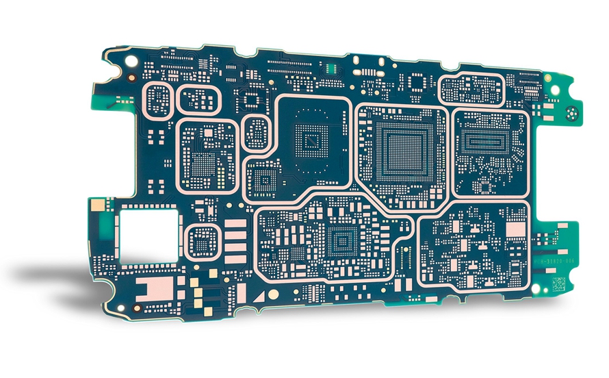
A Bare PCB is a printed circuit board without any electronic components mounted on it. Unlike an assembled PCB, a bare circuit board contains the fabricated conductive patterns, pads, vias, dielectric materials, solder mask, and other required features, but it does not yet contain components such as integrated circuits, resistors, capacitors, connectors, or switches.
A bare PCB is a fundamental building block of modern electronics manufacturing. It provides both the electrical interconnection and mechanical foundation required for subsequent PCB Assembly. Bare boards are used in prototypes, engineering validation, production testing, and mass manufacturing across industries ranging from consumer electronics and automotive systems to medical devices, industrial equipment, and aerospace electronics.
Understanding the structure, materials, manufacturing process, testing requirements, and applications of bare PCBs can help engineers and purchasing teams select the right board technology for their projects.
What Is a Bare PCB?
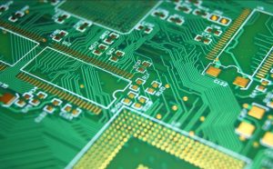
A bare PCB, also called a printed wiring board (PWB) in some contexts, is a fabricated circuit board that does not have electronic components installed.
During PCB Manufacturing, conductive copper patterns are formed on one or more layers of an insulating substrate. Depending on the board design, the PCB may also contain plated through-holes, blind vias, buried vias, microvias, solder mask, silkscreen, and surface finishes.
The resulting bare board is then supplied to the next manufacturing stage, where components can be attached through technologies such as surface-mount technology (SMT) or through-hole technology (THT).
It is useful to distinguish two related processes:
- PCB Manufacturing — fabricates the physical bare circuit board.
- PCB Assembly — installs and solders electronic components onto the bare PCB.
Therefore, a bare PCB is not simply a drawing or circuit layout. It is a physical, manufactured circuit board that is ready for component assembly.
For projects requiring custom dimensions, layer counts, materials, copper weights, impedance control, or surface finishes, Kingda can support bare PCB manufacturing according to project-specific design and production requirements.
Bare PCB vs. Assembled PCB: What Is the Difference?
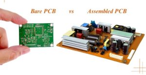
The main difference between a bare PCB and an assembled PCB is whether electronic components have been installed.
| Feature | Bare PCB | Assembled PCB |
|---|---|---|
| Components | No electronic components installed | Components are mounted and soldered |
| Function | Provides electrical interconnection and mechanical support but does not perform the complete system function | Performs its intended electronic function when powered and properly integrated |
| Manufacturing | PCB fabrication processes | PCB fabrication plus SMT/THT and other assembly processes |
| Cost | Generally lower because component and assembly costs are excluded | Higher because it includes components, labor, equipment, inspection, and assembly |
| Typical Use | Prototyping, PCB validation, fabrication testing, and production preparation | Functional products and electronic systems |
| Testing | Electrical and physical tests of the board itself | Functional, electrical, and assembly-level testing |
A bare PCB can therefore be considered the foundation of an assembled PCB. Before expensive components are installed, manufacturers can verify whether the fabricated board meets the required dimensional, electrical, and quality specifications.
What Is the Structure of a Bare PCB?
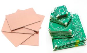
A bare PCB can be understood as a multilayer structure made from conductive and insulating materials. The exact construction depends on whether the board is single-sided, double-sided, multilayer, rigid, flexible, or rigid-flex.
Typical bare PCB features include the following.
Copper Layers
Copper is the primary conductive material in most PCBs. Copper foil is bonded to the substrate and patterned through imaging and etching or other circuit-forming processes.
The resulting copper features include:
- Signal traces
- Power and ground planes
- Component pads
- Copper pours
- Via structures
Copper thickness is selected according to current-carrying requirements, mechanical considerations, impedance requirements, and manufacturing capability.
Core Material
A PCB core is a fully cured dielectric material with copper foil laminated to one or both sides. In rigid PCBs, common core materials include FR-4-family laminates.
The core provides mechanical stability and electrical insulation between conductive layers.
Prepreg
Prepreg, short for pre-impregnated material, generally consists of woven glass reinforcement impregnated with partially cured resin.
During multilayer lamination, heat and pressure cause the resin to flow and cure, bonding copper layers and cores together into a unified PCB structure.
The thickness and dielectric characteristics of prepreg are important for multilayer stackup design and controlled-impedance applications.
Vias
Vias are plated holes or microstructures that electrically connect different conductive layers.
Common via types include:
- Through vias
- Blind vias
- Buried vias
- Microvias
Vias are particularly important in Multilayer PCB and HDI designs because they allow signals and power connections to transition between layers.
Solder Mask
The solder mask is the protective polymer coating applied over selected areas of the PCB surface.
Although green is the most common color, solder masks are also available in colors such as black, blue, red, white, and other options.
The solder mask helps:
- Protect exposed copper
- Reduce the risk of solder bridges
- Improve electrical insulation between exposed conductors
- Protect the board surface from environmental contamination
Importantly, component pads and other areas intended for soldering remain exposed.
Surface Finish
Exposed copper pads are typically protected with a surface finish to improve solderability and protect the copper from oxidation.
Common surface finishes include:
- HASL
- Lead-free HASL
- ENIG
- ENEPIG
- Immersion silver
- Immersion tin
- OSP
The appropriate finish depends on factors such as component pitch, assembly process, storage requirements, reliability targets, and cost.
Silkscreen
Silkscreen is the printed identification layer used for reference designators, polarity indicators, logos, labels, and other manufacturing or assembly information.
It is not electrically conductive and does not form part of the circuit itself.
Materials Commonly Used in Bare PCB Manufacturing
Material selection is one of the most important decisions in PCB Design and manufacturing.
Different applications require different combinations of dielectric performance, mechanical strength, thermal stability, flexibility, cost, and environmental resistance.
Two widely used substrate families are FR-4 and polyimide.
| Property | FR-4 | Polyimide |
|---|---|---|
| Material Type | Glass-reinforced epoxy laminate | Polyimide-based flexible dielectric |
| Mechanical Strength | High | Good, with excellent flexibility |
| Thermal Performance | Suitable for a wide range of general applications | Excellent thermal stability |
| Flexibility | Rigid in conventional constructions | Highly flexible |
| Typical Applications | Rigid PCBs | Flexible and rigid-flex PCBs |
| Relative Cost | Generally lower | Generally higher |
FR-4
FR-4 is a broad family of glass-reinforced epoxy laminate materials widely used for rigid PCBs.
Its combination of mechanical strength, electrical insulation, manufacturability, and cost makes it suitable for a broad range of electronic products.
Different FR-4 materials can have different Tg, Td, dielectric properties, thermal performance, and other characteristics, so engineers should select the specific laminate according to the application rather than treating all FR-4 materials as identical.
Polyimide
Polyimide is commonly used for flexible circuits because it provides a combination of flexibility, thermal stability, and chemical resistance.
It is particularly useful when the PCB must bend, fold, or fit into a mechanically constrained space.
Polyimide-based constructions are commonly found in:
- Flexible displays
- Cameras
- Medical electronics
- Wearable electronics
- Automotive electronics
- Compact consumer devices
Other PCB material families include high-frequency laminates, PTFE-based materials, metal-core laminates, ceramic substrates, and specialized low-loss materials.
PCB Standards for Bare PCB Manufacturing
Selecting a suitable PCB material is only one part of achieving reliable production. The board must also be manufactured according to appropriate design, material, and performance requirements.
Several IPC standards are commonly referenced in PCB manufacturing.
IPC-4101 covers material requirements for rigid and multilayer printed boards, while IPC-6012 establishes qualification and performance requirements for rigid printed boards. IPC-TM-650 provides standardized test methods used to evaluate various PCB characteristics.
The exact standards applicable to a project depend on the PCB type, industry, reliability class, and customer specification.
For high-reliability applications, engineers should define applicable standards during the design stage rather than treating standards compliance as a final inspection step.
Bare PCB Quality Testing and Inspection
Testing is a critical stage of Bare PCB Manufacturing because defects discovered after component assembly can lead to substantially higher rework and replacement costs.
Typical bare PCB inspection and testing methods include:
Automated Optical Inspection (AOI)
AOI systems use cameras and image-processing technology to inspect PCB features such as traces, pads, solder mask openings, component-related markings, and other fabricated patterns.
AOI is particularly useful for identifying manufacturing defects that can be detected visually.
Electrical Testing
Electrical testing verifies whether the fabricated conductive network matches the intended circuit connectivity.
Common approaches include:
- Flying-probe testing
- Fixture-based electrical testing
- Continuity testing
- Isolation testing
Electrical testing can identify open circuits and short circuits before the board proceeds to component assembly.
Dimensional Inspection
Manufacturers may inspect:
- Board dimensions
- Hole diameter
- Hole position
- Layer registration
- Copper thickness
- Board thickness
- Surface finish
- Warpage
Dimensional control becomes especially important for boards that must fit precisely into mechanical assemblies.
Surface Finish Inspection
The surface finish must provide reliable solderability and adequate protection for exposed copper.
Inspection may evaluate surface appearance, coating characteristics, thickness, and other parameters according to the selected finish and applicable specifications.
IPC-TM-650 Testing
IPC-TM-650 is a collection of standardized test methods used for evaluating various properties of printed boards and related materials.
The specific tests required depend on the board construction and customer requirements.
Testing bare PCBs before assembly helps prevent defective boards from consuming expensive components and assembly resources.
What Are the Different Types of Bare PCBs?
Bare PCBs can be classified according to layer count, construction, material, flexibility, and intended application.
Single-Sided PCB
A single-sided PCB contains one primary conductive copper layer.
Because of its relatively simple construction, it is generally economical and suitable for applications with lower routing density.
Typical applications include:
- Simple control circuits
- Power supplies
- Consumer products
- Basic industrial electronics
Double-Sided PCB
A double-sided PCB contains copper layers on both sides of the dielectric substrate.
Plated through-holes and vias allow electrical connections between the two sides, providing greater routing flexibility than a single-sided board.
Multilayer PCB
A multilayer PCB contains three or more conductive layers separated by dielectric materials.
Multilayer construction allows designers to achieve:
- Higher routing density
- Dedicated power and ground planes
- Better signal-routing flexibility
- More compact product designs
- Improved support for high-speed interfaces
Advanced multilayer designs may also incorporate blind vias, buried vias, and microvias.
Rigid PCB
Rigid PCBs use a mechanically stable substrate that does not normally bend during operation.
FR-4-based rigid boards are among the most widely used PCB constructions.
Flexible PCB
Flexible PCBs use flexible dielectric materials, commonly polyimide, allowing the circuit to bend or conform to a three-dimensional structure.
They are useful where conventional rigid boards would require excessive space or additional connectors.
Rigid-Flex PCB
Rigid-flex PCBs combine rigid sections with flexible circuit sections in one integrated construction.
This architecture can reduce connector count, save space, and support complex three-dimensional electronic assemblies.
Applications of Bare PCBs
Bare PCBs are used across virtually every major electronics industry.
Automotive Electronics
Modern vehicles contain numerous electronic control systems, including:
- Engine and powertrain control
- Battery management
- ADAS
- Infotainment
- Lighting
- Body control
- Sensor systems
- Communication systems
Depending on the application, automotive electronics may use rigid, flexible, or rigid-flex PCBs.
Medical Electronics
Medical equipment requires reliable electronic circuitry for sensing, control, monitoring, imaging, communications, and power management.
Bare PCBs may be used in:
- Patient monitoring equipment
- Diagnostic systems
- Medical imaging equipment
- Portable medical devices
- Laboratory equipment
- Surgical electronics
Material selection and PCB reliability requirements depend on the specific medical application and applicable equipment-level standards.
Consumer Electronics
Smartphones, laptops, tablets, cameras, televisions, networking devices, and other consumer products contain highly integrated PCBs.
Compact products frequently use multilayer, HDI, flexible, or rigid-flex technologies to accommodate high component density within limited physical space.
Aerospace and Defense Electronics
Aerospace electronics can require stringent control of reliability, mechanical durability, thermal performance, and traceability.
PCBs used in these environments may need to withstand demanding temperature cycling, vibration, shock, and long operating periods.
Industrial Electronics
Industrial automation equipment, robotics, motor controllers, instrumentation, PLC systems, power electronics, and factory-control systems rely heavily on PCBs.
Depending on the application, boards may need enhanced thermal management, mechanical durability, electrical isolation, or environmental protection.
Bare PCB for Prototyping and Product Development
One of the most important uses of a bare PCB is engineering prototyping.
During product development, engineers may use prototype bare boards to validate:
- PCB layout
- Component footprints
- Routing
- Power distribution
- Signal integrity
- Mechanical dimensions
- Connector locations
- Thermal considerations
- Manufacturing feasibility
Using a prototype PCB allows designers to identify issues before committing to large-scale production.
For example, if a prototype reveals that a connector interferes with the enclosure, the PCB layout can be modified before a large quantity of boards is assembled.
Advantages of Using Bare PCBs
Bare PCBs provide several important advantages during electronics development and manufacturing.
Lower Initial Cost
Because bare boards do not include electronic components or assembly labor, their initial unit cost is generally lower than that of completed PCB assemblies.
Easier Design Validation
Engineers can validate the fabricated board before committing expensive components to the assembly process.
Reduced Assembly Risk
Testing the bare PCB first can help identify manufacturing defects before components are installed.
Flexible Prototyping
Bare boards can be produced in prototype quantities for engineering verification, design iterations, and pre-production testing.
Suitable for Different Assembly Strategies
Once the bare PCB has been validated, it can proceed to SMT, THT, mixed-technology, or other assembly processes according to the product requirements.
How to Choose the Right PCB Manufacturer
Choosing a reliable bare PCB manufacturer requires more than comparing unit prices.
Consider the following factors:
- Manufacturing capabilities — Verify whether the manufacturer can produce the required layer count, board thickness, copper weight, hole sizes, materials, and surface finishes.
- Quality systems and standards — Review applicable certifications and quality-control procedures.
- Testing capabilities — Confirm that the manufacturer can perform required electrical, dimensional, visual, and reliability testing.
- Material control — Check whether the manufacturer can provide the required laminate and material specifications.
- Manufacturing experience — Consider experience with the specific PCB technology required by your project.
- Prototype and volume capability — Make sure production capacity matches both prototype and mass-production requirements.
- Engineering support — DFM review and engineering feedback can help identify manufacturing risks before production.
- Traceability — For demanding applications, material and production traceability can be an important requirement.
- Lead time — Evaluate whether the manufacturer’s production schedule can support your product-development timeline.
- Total cost — Compare the complete cost of manufacturing, testing, shipping, and potential quality issues rather than selecting a supplier based solely on the lowest quotation.
Kingda Bare PCB Manufacturing Support
Kingda can support customers with customized Bare PCB Manufacturing for different electronic applications, from prototype development to production requirements.
Depending on project specifications, the manufacturing process can be configured around factors such as:
- Single-sided, double-sided, and multilayer PCB structures
- Rigid, flexible, and rigid-flex constructions
- Different copper thicknesses
- Custom board dimensions
- Various dielectric materials
- Controlled-impedance requirements
- Different via structures
- Multiple surface finishes
- SMT/THT assembly requirements
- Electrical and visual inspection
For a new project, providing complete fabrication data—including Gerber files, drill files, stackup information, material requirements, copper weights, surface finish, and applicable specifications—can help the manufacturer evaluate manufacturability and provide an accurate quotation.
Conclusion
A Bare PCB is much more than an empty circuit board. It is a fully fabricated electronic interconnection platform that provides the physical structure and conductive pathways required for component assembly.
From single-sided boards used in simple circuits to advanced multilayer, flexible, rigid-flex, and HDI structures, bare PCBs support a wide range of electronic products.
A reliable bare PCB manufacturing process requires careful control of materials, layer structures, copper features, vias, surface finishes, dimensions, and electrical performance. Proper inspection and testing before assembly can also reduce manufacturing risk and prevent defective boards from progressing into more expensive PCBA processes.
For engineers and purchasing teams, selecting the right PCB Design, materials, manufacturing technology, testing strategy, and supplier is essential for achieving reliable and cost-effective electronic products.