Radar PCB Design & PCB Manufacturing: Materials, Frequency, Applications & Manufacturing Guide
Have you ever wondered how vehicles detect obstacles in dense fog, how aircraft and missiles can be detected over large areas, or how security systems sense movement without relying on cameras? The answer is radar technology. At the heart of these systems is a highly specialized Radar PCB designed to transmit, receive, and process high-frequency signals with exceptional precision.
Radar, short for Radio Detection and Ranging, works by transmitting electromagnetic waves and analyzing the signals reflected from surrounding objects. A Radar PCB provides the electrical foundation required to generate, route, receive, amplify, and process these high-frequency signals.
Unlike conventional circuit boards, radar boards must maintain extremely consistent electrical characteristics. Even a small variation in trace geometry, dielectric thickness, impedance, or material properties can affect signal integrity and ultimately influence radar detection accuracy.
For this reason, Radar PCB Design requires careful consideration of materials, controlled impedance routing, antenna structures, grounding, electromagnetic compatibility (EMC), thermal management, and manufacturing tolerances. These requirements become even more demanding in automotive, aerospace, defense, industrial, and medical applications.
What Is a Radar PCB?

A Radar PCB is a specialized printed circuit board designed to support the high-frequency transmission, reception, and processing functions of a radar system.
The basic radar process is relatively straightforward: a radar system transmits an RF signal, the signal travels through the environment, and objects reflect part of that energy back toward the receiver. The radar electronics then analyze the returned signal to determine information such as:
- Target presence
- Distance
- Direction
- Relative velocity
- Movement
- Target position
The Radar PCB integrates many of the electronic circuits required to perform these functions within a compact structure.
A typical radar board may include an RF transceiver, transmission and reception circuitry, antennas or antenna interfaces, filters, amplifiers, power-management circuits, microcontrollers, and digital signal-processing components.
The RF transceiver generates and receives high-frequency signals, while the antenna structure transmits electromagnetic energy and captures reflected signals. A microcontroller, digital signal processor (DSP), or dedicated radar processing device then analyzes the received information.
Power-management circuits provide stable voltage and current to the different functional blocks. High-quality grounding and decoupling are also essential because noise generated by digital circuits can interfere with sensitive RF circuitry.
Today, Radar PCB Manufacturing supports a wide range of applications, including automotive radar, industrial automation, robotics, smart-home presence detection, security systems, aerospace equipment, and non-contact medical monitoring.
Radar PCB Frequency Range
The frequency range of a radar PCB depends on the radar architecture and application. Modern radar systems can operate from the low-GHz range to millimeter-wave frequencies, with automotive radar commonly using bands around 24 GHz and 77–81 GHz.
At these frequencies, PCB design becomes significantly more sensitive to physical geometry and material characteristics.
As operating frequency increases, several effects become increasingly important:
- Transmission-line impedance variations
- Dielectric loss
- Conductor loss
- Skin effect
- Crosstalk
- Electromagnetic interference (EMI)
- Signal reflection
- Via discontinuities
- Connector losses
- Antenna coupling
Therefore, High Frequency PCB technology used in radar applications requires much tighter control than many conventional digital PCB designs.
Material selection is especially important. The dielectric constant (Dk) and dissipation factor (Df) of the laminate influence propagation velocity, impedance, phase characteristics, and insertion loss.
Radar PCBs may also be deployed in demanding environments, including vehicles, industrial facilities, aircraft, satellites, and defense systems. Consequently, electrical performance must be combined with mechanical reliability, thermal stability, and long-term environmental resistance.
Key Requirements for Radar PCB Design
Radar PCB Design is considerably more demanding than conventional PCB design because the circuit operates at high frequencies and often performs safety- or mission-critical functions.
Controlled Impedance Routing
Controlled impedance is one of the most important requirements in radar PCB design.
RF transmission lines must maintain a predictable characteristic impedance along their entire signal path. A commonly used RF impedance is 50 ohms, although the actual target depends on the system architecture and interface requirements.
Changes in trace width, copper thickness, dielectric thickness, dielectric constant, or reference-plane geometry can alter impedance.
An impedance discontinuity can cause signal reflections, insertion loss, phase errors, and reduced power transfer.
For this reason, RF traces should be carefully calculated and verified during both design and PCB Manufacturing.
Low-Loss PCB Materials
Conventional FR-4 materials are widely used for general-purpose PCBs, but they may not provide the low dielectric loss required for many high-frequency and millimeter-wave applications.
Specialized materials from manufacturers such as Rogers, Isola, and Taconic can provide controlled dielectric properties and lower signal losses.
For demanding radar designs, engineers should evaluate:
- Dielectric constant (Dk)
- Dissipation factor (Df)
- Thermal stability
- Moisture absorption
- Copper surface characteristics
- Coefficient of thermal expansion (CTE)
- Laminate thickness tolerance
The correct material should always be selected according to the actual operating frequency, stackup, transmission-line geometry, environmental conditions, and manufacturing process.
Antenna Design and Placement
The antenna is another critical part of a radar PCB.
Depending on the system architecture, the antenna may be integrated directly into the PCB using microstrip, patch, or other planar antenna structures, or it may be implemented as a separate antenna module.
Antenna geometry, spacing, substrate properties, copper pattern accuracy, and surrounding structures can all affect antenna performance.
The antenna area should therefore be carefully isolated from noisy digital circuitry, power components, mechanical structures, and other sources of electromagnetic interference.
Grounding and Shielding
A well-designed ground structure provides a controlled return path for high-frequency currents and helps reduce unwanted coupling.
Radar boards may use dedicated ground planes, ground stitching vias, shielding structures, and carefully controlled signal-layer transitions.
However, grounding must be designed according to the antenna architecture. A solid ground plane can be beneficial beneath RF transmission lines while being inappropriate directly beneath certain PCB-integrated antenna structures.
Thermal Management
Radar electronics can generate considerable heat, particularly when high-performance RF transceivers, power amplifiers, processors, and other active components operate continuously.
Thermal management may include:
- Thermal vias
- Copper planes
- Heat spreaders
- Metal-backed structures
- External heat sinks
- Thermally optimized component placement
Thermal design is particularly important in automotive and industrial radar applications, where the PCB may experience wide temperature variations.
Radar PCB Design Considerations
A reliable Radar PCB Design requires careful coordination between electrical engineering, mechanical engineering, materials engineering, and manufacturing.
1. Select an Appropriate PCB Stackup
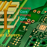
The layer stackup determines the physical relationship between signal layers, reference planes, power layers, and dielectric materials.
A radar board may require multiple dedicated ground planes to separate sensitive RF circuits from high-speed digital circuitry.
For more advanced designs, a hybrid stackup may combine low-loss RF laminates with conventional FR-4 materials. This approach can provide the required RF performance while controlling overall manufacturing cost.
However, hybrid constructions require careful analysis of:
- Material compatibility
- CTE
- Lamination behavior
- Dielectric thickness
- Registration
- Manufacturing tolerances
2. Select the Right Materials
There is no universal PCB material that is ideal for every radar application.
Standard FR-4 can be suitable for certain lower-frequency or short RF interconnects, particularly when trace lengths are short and loss requirements are moderate. However, higher-frequency radar applications often require specialized low-loss laminates.
Engineers should consult manufacturer datasheets and evaluate material performance at the actual operating frequency rather than selecting a material based solely on its nominal Dk value.
3. Control Impedance and Signal Length
RF traces commonly use 50-ohm controlled impedance, but the correct impedance should always be determined by the system interface.
High-speed digital interfaces may use differential impedance according to their communication standards.
Trace geometry should remain consistent wherever possible. Unnecessary layer transitions, abrupt width changes, sharp discontinuities, and excessive vias should be minimized in sensitive RF paths.
4. Maintain a Continuous Return Path
High-frequency signals require a predictable return-current path.
A continuous reference plane beneath a transmission line helps reduce loop area and electromagnetic radiation. Ground stitching vias can also be used to control electromagnetic fields and improve isolation between functional areas.
Designers should avoid routing high-speed signals across gaps or splits in their reference planes because doing so can force return currents to take longer paths.
5. Protect the Antenna Region
One of the most important rules in antenna-integrated radar PCB design is to maintain the manufacturer’s specified antenna keep-out region.
Unintended copper, ground planes, components, mechanical structures, or conductive materials near an antenna can change its electromagnetic characteristics.
Therefore, the antenna layout should be designed together with the mechanical enclosure and final product structure rather than treating the PCB as an isolated component.
Radar PCB vs. Standard High-Frequency PCB
Radar PCBs and standard High Frequency PCBs share many design principles, but their performance requirements can differ significantly.
| Parameter | Radar PCB | Standard High-Frequency PCB |
|---|---|---|
| Primary purpose | Designed specifically for transmitting, receiving, and processing radar signals | Designed for high-speed or RF signal transmission in general electronic systems |
| Typical applications | Automotive radar, aerospace, defense, industrial sensing, surveillance | Wireless communication, Wi-Fi, networking, RF equipment, instrumentation |
| Frequency | May operate from several GHz into the millimeter-wave range | Can range from low GHz to much higher frequencies depending on the application |
| Material requirements | Often requires low-loss materials with tightly controlled dielectric properties | Material selection depends on frequency, loss, cost, and application |
| Impedance control | Often extremely critical, particularly for RF paths and antenna interfaces | Important but may allow broader design margins depending on application |
| Antenna integration | Frequently integrated directly into the PCB or closely coupled to the board | May use separate antennas or RF connectors |
| Signal loss tolerance | Often very low because loss and phase errors can affect detection performance | Depends on system requirements |
| Manufacturing tolerance | Tight control may be required for RF geometry and antenna structures | Depends on design complexity and operating frequency |
The distinction is therefore not simply the operating frequency. Radar PCB Manufacturing must consider the complete RF system, including antenna performance, signal integrity, phase stability, impedance control, thermal behavior, and environmental reliability.
Radar PCB Manufacturing Process
The Radar PCB Manufacturing process requires tighter process control than many standard circuit boards.
1. Material Selection
The first step is selecting laminate materials according to the required frequency, dielectric properties, thermal requirements, and mechanical structure.
Common material families for high-frequency applications include PTFE-based laminates and hydrocarbon/ceramic systems.
Materials from Rogers, Isola, and Taconic are frequently considered for demanding RF applications.
2. PCB Layout and Engineering Review
Before fabrication begins, engineers create the PCB layout using professional CAD software.
The design should include:
- Controlled impedance requirements
- RF transmission-line geometry
- Antenna dimensions
- Grounding strategy
- Power distribution
- Thermal management
- Component placement
- Layer stackup
- Manufacturing tolerances
A DFM review should also be performed before releasing the design for production.
3. Inner-Layer Imaging
For multilayer radar PCBs, the inner-layer circuit patterns are transferred onto copper-clad laminates using imaging processes.
High-resolution imaging is particularly important for fine RF structures and controlled transmission-line geometries.
4. Etching
Unwanted copper is removed through a controlled etching process, leaving the required circuit patterns.
Trace width and spacing must be carefully controlled because variations can affect transmission-line impedance and signal performance.
5. Lamination
The individual layers are aligned and laminated using heat and pressure.
Proper lamination is essential for maintaining dielectric thickness, layer registration, and mechanical integrity.
For RF applications, voids, delamination, excessive resin variation, and layer misalignment can negatively affect electrical performance.
6. Drilling and Via Formation
Drilling creates through-holes and other interconnection structures used to connect PCB layers.
Depending on the design, mechanical drilling or laser drilling may be used.
For high-density radar boards, small vias and carefully controlled via structures can help reduce parasitic effects and preserve signal integrity.
7. Surface Finish and Solder Mask
The exposed copper is protected using an appropriate surface finish.
ENIG is one possible option, particularly where flat pads and good solderability are required. However, the optimal finish depends on the component technology, RF structure, reliability requirements, and manufacturing process.
A solder mask is also applied to protect exposed copper and reduce the risk of solder bridging and contamination.
For PCB-integrated antenna structures, solder mask coverage must be considered during RF design because the additional dielectric layer can affect antenna characteristics.
8. Testing and Quality Control
Every high-quality radar PCB should undergo appropriate inspection and testing before shipment.
Depending on the application, testing may include:
- Automated optical inspection (AOI)
- Electrical testing
- Controlled impedance testing
- Dimensional inspection
- Microsection analysis
- Solderability testing
- Surface-finish inspection
- X-ray inspection
- Signal-integrity verification
For demanding applications, Kingda can incorporate appropriate inspection and quality-control procedures into the manufacturing process according to project requirements.
Materials Used in Radar PCB Manufacturing
Material selection is one of the most important decisions in Radar PCB Manufacturing because laminate characteristics directly affect RF performance.
RO4350B
RO4350B is a widely used high-frequency laminate from Rogers. It combines relatively low loss with a manufacturing process that is compatible with many conventional PCB fabrication techniques.
Its nominal dielectric constant and loss characteristics make it suitable for a wide range of RF and microwave applications.
It can also be used in hybrid constructions where RF performance is required in selected layers while conventional PCB materials are used elsewhere.
RO3003
RO3003 is a ceramic-filled PTFE laminate designed for demanding RF and microwave applications.
It provides very low dielectric loss and stable electrical characteristics, making it suitable for applications where signal attenuation and phase stability are important.
The material can be considered for advanced radar and microwave designs, although material cost and manufacturing requirements should be evaluated carefully.
Astra MT77
Astra MT77 is a high-performance laminate from Isola designed for high-frequency applications.
Its low-loss characteristics and thermal performance make it a potential choice for demanding RF and millimeter-wave applications, including automotive radar designs.
The actual suitability should be evaluated according to the target frequency, stackup, operating temperature, and fabrication process.
Taconic RF-35
Taconic RF-35 is another laminate used in high-frequency RF applications.
Its low-loss characteristics can make it suitable for RF transmission lines, antennas, and radar-related circuits where maintaining signal integrity is important.
The final material selection should always be based on verified electrical specifications at the intended operating frequency.
Applications of Radar PCBs
Radar technology has expanded well beyond traditional military and aerospace applications. Modern Radar PCBs are now used in automotive, industrial, consumer, security, and medical systems.
FMCW Radar
Frequency-Modulated Continuous-Wave (FMCW) radar continuously transmits signals whose frequency changes over time.
It can be used to determine target range and velocity and is widely used in automotive radar and other sensing applications.
Doppler Radar
Doppler radar uses frequency shifts caused by relative motion to estimate target velocity.
It is commonly used in motion detection, speed measurement, industrial sensing, and other applications.
Pulse Radar
Pulse radar transmits short electromagnetic pulses and measures the time required for reflected signals to return.
This architecture is commonly associated with long-range detection and surveillance applications.
Synthetic Aperture Radar (SAR)
Synthetic Aperture Radar uses the motion of a radar platform to create high-resolution images.
SAR systems are used in satellites, aircraft, Earth observation, mapping, environmental monitoring, and other applications.
MIMO Radar
Multiple-Input Multiple-Output (MIMO) radar uses multiple transmit and receive channels to improve spatial resolution and target detection capabilities.
MIMO radar is increasingly important in automotive sensing systems because multiple antennas can provide more information about the surrounding environment.
How to Choose a Radar PCB Manufacturer
Selecting an experienced Radar PCB Manufacturer is an important part of developing a reliable radar product.
A capable supplier should understand not only standard PCB fabrication but also high-frequency materials, controlled impedance, RF layout requirements, antenna structures, and manufacturing tolerances.
1. Evaluate High-Frequency PCB Experience
Start by examining the manufacturer’s experience with RF and microwave PCB projects.
A manufacturer should understand the relationship between PCB geometry, dielectric properties, impedance, and RF performance.
Experience with radar-related projects can also be valuable when dealing with antenna-integrated boards and millimeter-wave applications.
2. Check Quality Certifications and Standards
Review the manufacturer’s applicable quality-management certifications and industry standards.
Depending on the application, relevant qualifications may include ISO 9001 and applicable IPC standards.
For automotive, aerospace, medical, or other regulated applications, additional industry-specific requirements may apply.
3. Verify Material Capabilities
Confirm that the manufacturer can process the materials required for your design.
This may include specialized Rogers, Isola, Taconic, PTFE-based, ceramic-filled, or hybrid laminates.
The supplier should also understand the lamination, drilling, plating, and finishing requirements associated with these materials.
4. Review Impedance-Control Capabilities
Controlled impedance is critical for radar PCBs.
Ask whether the manufacturer provides impedance calculation, test coupons, impedance testing, and process monitoring.
The manufacturer should be able to correlate the designed transmission-line geometry with the actual fabricated PCB.
5. Evaluate Inspection and Testing
A radar PCB manufacturer should have appropriate inspection and testing capabilities.
Depending on the project, these may include AOI, electrical testing, X-ray inspection, dimensional measurement, impedance testing, and microsection analysis.
6. Consider Engineering Support
A strong manufacturing partner should be able to identify potential DFM issues before production.
Kingda can work with customers on PCB manufacturing requirements, material selection, stackup considerations, impedance control, production documentation, and quality inspection according to project specifications.
7. Evaluate Production Capacity and Delivery
Finally, consider whether the manufacturer can support your required prototype quantities, mass-production volumes, lead times, and quality requirements.
For radar applications, production speed should not come at the expense of process control and consistency.
Why Radar PCB Design and Manufacturing Require Precision
Radar systems depend on accurately transmitting and receiving electromagnetic signals.
A conventional PCB error that appears insignificant at low frequency can become much more important at millimeter-wave frequencies.
For example, variations in:
- Trace width
- Dielectric thickness
- Copper roughness
- Via dimensions
- Layer registration
- Antenna geometry
- Connector positioning
can influence RF performance.
This is why successful radar electronics require close coordination between PCB Design, RF engineering, antenna engineering, mechanical design, and PCB Manufacturing.
The PCB is not simply a platform for mounting components. At high frequencies, the physical structure of the PCB becomes part of the electrical system itself.
Conclusion
A Radar PCB is one of the most technically demanding types of printed circuit board because it must support high-frequency signal transmission, reception, processing, and often antenna integration within a compact and highly controlled structure.
Successful radar board development depends on several interconnected factors, including low-loss materials, controlled impedance, appropriate layer stackup, antenna design, grounding, shielding, thermal management, and precise manufacturing.
As radar technology continues to expand into automotive safety, autonomous driving, industrial automation, robotics, aerospace, security, and medical sensing, the demand for high-performance Radar PCB Manufacturing.
For companies developing radar products, selecting an experienced manufacturing partner such as Kingda can help establish a reliable production process from engineering review and material selection through fabrication, inspection, and delivery.