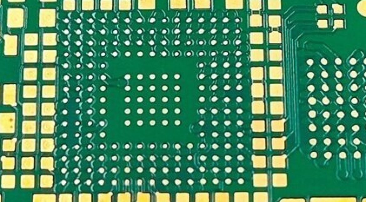
Microvia PCB Technology: PCB Design, PCB Manufacturing, Types, Benefits & Design Guidelines
The invention of microvia technology has fundamentally changed the way modern electronic circuits are designed and manufactured. As electronic products continue to become smaller, faster, and more functionally integrated, conventional through-hole interconnects can consume valuable board space and limit routing density. Microvia PCB technology provides an effective solution by enabling compact layouts, higher interconnection density, improved signal integrity, and more efficient use of multilayer structures.
Microvias are particularly important in HDI PCB technology, where extremely small interconnections allow engineers to route more signals within a limited board area. From smartphones and wearable devices to automotive electronics, telecommunications equipment, and medical devices, microvia technology has become an important part of advanced PCB Design and PCB Manufacturing.
This article explains what microvias are, how microvia PCBs are manufactured, their major types and benefits, key design guidelines, applicable IPC standards, manufacturing challenges, and common applications.
What Is a Microvia and What Is a Microvia PCB?
A microvia is a very small plated interconnection used to connect adjacent conductive layers in a multilayer PCB. Unlike a conventional through-hole via, a microvia normally does not extend through the entire thickness of the circuit board.
Microvias are commonly formed using laser drilling and are especially important in HDI PCB structures. Their small dimensions allow designers to place vias closer together and position them within or near component pads, creating additional routing channels that would not be practical with conventional vias.
Depending on the stack-up and manufacturing process, microvias can be arranged as blind, buried, stacked, or staggered structures.
A Microvia PCB is therefore a circuit board incorporating one or more microvia structures to achieve higher wiring density, more compact component placement, and improved interlayer connectivity.
What Is a Microvia According to IPC Standards?
The definition of a microvia should be distinguished from general small-diameter vias. IPC terminology and HDI design standards define microvias based on factors such as their diameter, depth, and aspect ratio.
For practical HDI manufacturing, designers commonly target a microvia aspect ratio of approximately 1:1 or lower, although the exact acceptable value depends on the material system, drilling process, copper plating capability, via diameter, and reliability requirements.
Microvia depth is also an important parameter. Shallow microvias generally provide better plating reliability because copper deposition inside the hole is easier to control.
It is important not to treat a single aspect-ratio value as a universal manufacturing rule. The applicable requirements should be confirmed against the latest relevant IPC standard, material datasheet, and the PCB manufacturer’s process capability.
What Is Microvia PCB Technology?
Microvia PCB Technology refers to the design and manufacturing techniques used to create extremely small interlayer connections, typically using laser drilling and controlled copper plating.
A laser creates a small opening through the dielectric material, after which the exposed structure is prepared and copper is deposited to form a reliable electrical connection. In advanced HDI manufacturing, microvias may also be filled with copper and subsequently capped or stacked to create more sophisticated interconnection structures.
The primary purpose of microvia technology is to increase routing density without continuously increasing PCB dimensions. Because microvias can be significantly smaller and shallower than conventional through-hole vias, they provide PCB designers with additional routing flexibility.
Microvias can also reduce via stubs and shorten signal paths, which can be beneficial for high-speed digital and RF designs when the overall stack-up and signal-routing strategy are properly engineered.
Understanding the Fundamentals of Microvia Technology
The growing demand for smaller and more powerful electronic devices has accelerated the adoption of microvia technology. Modern products often require more components, higher data rates, and greater functionality within increasingly limited physical dimensions.
Microvias act as electrical bridges between conductive layers in an HDI PCB. They can carry high-speed signals, power, and ground connections while occupying considerably less board area than traditional through-hole vias.
A typical microvia is formed between adjacent layers and may be configured as a blind microvia. Multiple microvias can then be combined into stacked or staggered structures to support more complex HDI architectures.
This approach enables engineers to:
- Increase routing density
- Reduce via size and pad requirements
- Shorten electrical interconnection paths
- Improve component placement flexibility
- Reduce PCB size
- Support fine-pitch components
- Build more compact multilayer circuits
Types of Microvias Used in PCB Design
Microvias can be categorized according to their electrical connection, position within the stack-up, and manufacturing structure.
1. Blind Microvias
A blind microvia connects an outer conductive layer to one or more internal layers without passing completely through the PCB.
This structure allows designers to use internal routing space more efficiently while keeping the opposite side of the PCB available for additional circuitry.
2. Buried Microvias
A buried microvia connects internal conductive layers without being directly exposed on the outer surface of the PCB.
Because the connection is contained within the board structure, buried microvias can provide additional routing resources while preserving valuable surface area.
3. Through-Hole Vias
Traditional through-hole vias extend through the complete PCB thickness. They are not normally classified as microvias simply because their diameter is small.
However, through-hole vias remain an important reference point when comparing microvia structures because they consume more vertical space and can create larger routing obstacles in high-density designs.
4. Stacked Microvias
Stacked microvias are vertically aligned across multiple adjacent layers. One microvia is positioned directly above another, allowing an interconnection to span several layers.
Stacked structures can provide excellent routing density, but they require highly controlled manufacturing processes. Copper filling and reliable interconnection between stacked structures are particularly important.
5. Staggered Microvias
Staggered microvias are offset from one another rather than vertically aligned.
Compared with stacked structures, staggered configurations can simplify certain manufacturing processes and reduce some of the reliability challenges associated with vertically stacked microvias.
The choice between stacked, staggered, and other microvia structures depends on the PCB stack-up, routing requirements, component density, reliability target, and manufacturer’s process capability.
Why Are Microvias Important in Modern Electronics?
As electronic products become smaller and more sophisticated, available PCB real estate becomes increasingly valuable. Microvia technology enables designers to use this limited space more efficiently.
Microvias are particularly valuable for smartphones, wearable electronics, compact computing systems, automotive electronics, medical devices, and telecommunications equipment.
Their smaller geometry allows components to be placed more densely while providing additional routing channels between layers.
For high-speed designs, microvias can also reduce unnecessary via stubs and shorten interconnect paths. When combined with appropriate impedance control, stack-up planning, grounding, and signal-integrity techniques, this can help support high-speed electrical performance.
In short, microvias are one of the enabling technologies behind modern HDI PCB and multilayer PCB designs.
Major Benefits of Microvia PCB Technology
1. Improved Signal Performance and Routing Efficiency
One of the major advantages of microvias is their ability to shorten electrical interconnection paths.
A properly designed microvia structure can reduce unnecessary via stubs and parasitic effects compared with conventional interconnect structures. This is particularly valuable in high-speed digital and RF applications where signal integrity is sensitive to discontinuities.
Higher Bandwidth
Microvias occupy less physical space and can support dense routing around fine-pitch components. Their reduced geometry can also help engineers design shorter signal paths for demanding high-frequency applications.
Better Thermal Management
Microvias can also contribute to thermal management when appropriately designed as thermal via structures.
For power electronics and high-density components, arrays of small vias can help transfer heat from component regions into internal or opposite-side copper structures. Thermal performance, however, depends on the complete PCB stack-up, copper thickness, via filling, substrate material, and heat-spreading design.
2. Space-Saving PCB Design
Space efficiency is one of the strongest reasons to use microvias.
Because microvias are significantly smaller than many conventional via structures, designers can place routing channels in areas that would otherwise be consumed by larger pads and clearances.
Smaller PCB Footprint
Portable products require smaller and lighter electronics. Microvias make it possible to increase circuit density without proportionally increasing board dimensions.
This is particularly useful in smartphones, smartwatches, wearable devices, compact medical equipment, and miniature sensors.
More Efficient Layer Utilization
Microvias allow connections to be made between selected layers rather than forcing a connection through the complete PCB thickness.
This provides greater freedom when building complex PCB Stackup structures and can reduce routing congestion.
3. Potential Material and System Cost Benefits
Microvia technology can reduce PCB size and improve material utilization. A smaller board may require less laminate and copper area, while increased routing density can sometimes reduce the need for additional board layers.
However, microvia manufacturing itself requires advanced equipment, tighter process control, laser drilling, and potentially copper-filled structures. Therefore, microvia technology should not automatically be considered cheaper than conventional PCB manufacturing.
The overall cost depends on board size, layer count, material selection, via structure, production volume, yield, and manufacturing requirements.
4. High Reliability and Durability
When properly designed and manufactured, microvias can provide reliable interlayer connections.
Shallow microvias generally have a lower aspect ratio than deep conventional vias, making copper plating and thermal-mechanical stress management more controllable.
Reliability still depends heavily on material selection, copper plating quality, via geometry, thermal cycling, stacking strategy, and manufacturing consistency.
Microvia Manufacturing Technologies
Different technologies can be used to create small holes and interconnections, but they are not equally common in commercial HDI PCB manufacturing.
1. Laser Drilling
Laser drilling is the dominant method for producing microvias in modern HDI manufacturing.
UV and CO₂ laser systems can selectively remove dielectric material with high positional accuracy. Depending on the material structure, laser parameters can be optimized to create controlled microvia openings without unnecessarily damaging the underlying copper.
Major advantages include:
- High precision
- Small hole diameters
- High production flexibility
- Fast processing
- Suitable for HDI structures
- Excellent compatibility with fine-pitch designs
2. Mechanical Drilling
Mechanical drilling is widely used for conventional PCB holes, but it is not normally the primary method for true microvia formation.
Mechanical drilling can still be used for small conventional vias and other PCB holes where the required diameter and aspect ratio fall within the capabilities of the drilling equipment.
Therefore, mechanical drilling should not automatically be described as a standard microvia manufacturing method.
3. Electrical Discharge Machining (EDM)
Electrical discharge machining can create extremely precise features in suitable conductive materials. However, EDM is not a mainstream method for producing microvias in conventional multilayer PCB manufacturing.
It is more relevant to specialized microfabrication and applications requiring unusual material or geometric characteristics.
4. Advanced Additive and Printing Technologies
Inkjet printing, additive manufacturing, and other emerging processes are being investigated for advanced electronics manufacturing.
These approaches may provide opportunities for material-efficient manufacturing and novel interconnect structures. However, they should be distinguished from established high-volume microvia production methods such as laser drilling.
Microvia PCB Manufacturing Process
The manufacturing process for a Microvia PCB shares many stages with conventional multilayer PCB production, but it requires additional process control for laser drilling, desmear, copper plating, and via filling.
1. Initial PCB Design and Layout
The manufacturing process begins with detailed circuit design and layout.
Engineers must define the layer stack-up, component placement, routing strategy, microvia diameter, pad geometry, via depth, and electrical requirements.
A PCB Design tool is then used to perform Design Rule Checks (DRC) and verify that the design complies with the manufacturer’s manufacturing capabilities.
For HDI designs, engineers should establish microvia rules at the beginning of the project rather than trying to introduce microvias after the routing has already been completed.
2. Material Selection
Material selection has a direct influence on microvia reliability and manufacturing yield.
Important considerations include:
- Dielectric material
- Resin system
- Copper foil thickness
- Dielectric thickness
- Coefficient of thermal expansion
- Glass transition temperature
- High-frequency electrical properties
- Thermal performance
The material stack-up should be selected together with the microvia structure because laser drilling performance depends strongly on dielectric thickness and material composition.
3. Layer Formation and Lamination
The inner circuit layers are patterned and processed before multilayer lamination.
Prepreg or other bonding materials are used to form the multilayer structure. Heat and pressure are carefully controlled to achieve reliable bonding and dimensional stability.
For HDI boards, sequential lamination may be used to build additional layers and microvia structures in stages.
4. Laser Drilling
After the appropriate dielectric layer has been formed, laser drilling creates the microvia openings.
The laser parameters must be carefully controlled according to the dielectric material, copper thickness, hole diameter, and target depth.
5. Desmear and Surface Preparation
After drilling, residues can remain inside or around the microvia.
Desmear and cleaning processes remove unwanted resin residues and prepare the surface for reliable copper deposition.
Proper surface preparation is essential because poor adhesion can result in voids, weak plating, or premature microvia failure.
6. Copper Plating
Copper is deposited onto the prepared microvia surfaces to create an electrically conductive path.
Electroless copper deposition is commonly used as an initial conductive layer, followed by electrolytic copper plating to build the required copper thickness.
The plating process must provide sufficient coverage inside the microvia to maintain electrical and mechanical reliability.
7. Via Filling
For stacked microvia structures, copper filling is often particularly important.
A properly filled microvia can provide a flat surface for subsequent processing and enable another microvia to be formed above it.
Poor filling can create voids or weak regions that become reliability risks during thermal cycling and assembly.
8. Circuit Imaging and Etching
Photoresist is applied to the copper surface and patterned using imaging technology. After exposure and development, unwanted copper is removed through controlled etching.
This creates the desired conductive traces and pads.
The process must maintain accurate line width, spacing, registration, and copper geometry to support the high-density requirements of HDI designs.
9. Solder Mask and Surface Finish
A solder mask is applied to protect conductive areas and prevent unintended solder bridging.
The exposed pads then receive an appropriate surface finish, such as ENIG, ENEPIG, immersion silver, immersion tin, or HASL, depending on the application and assembly requirements.
Surface-finish selection is particularly important for fine-pitch components and microvia-in-pad structures.
Major Challenges in Microvia PCB Manufacturing
Although microvia technology offers significant advantages, it also introduces manufacturing challenges.
1. Design Complexity
Modern HDI designs can contain extremely dense routing, fine-pitch components, multiple microvia structures, and complicated stack-ups.
Designers must establish clear rules for via diameter, pad size, spacing, layer transitions, impedance, thermal requirements, and manufacturing tolerances.
2. Manufacturing Complexity
Microvia manufacturing requires precise laser drilling, reliable copper deposition, accurate registration, and controlled via filling.
A small variation in drilling depth, copper thickness, or layer alignment can affect the final interconnection.
3. Registration and Dimensional Stability
HDI manufacturing involves multiple layers and sequential processing steps. Thermal expansion, material movement, lamination pressure, and moisture can influence dimensional stability.
Maintaining accurate layer-to-layer registration is therefore essential.
4. Reliability and Process Control
Microvia structures may experience mechanical and thermal stresses during PCB fabrication, soldering, assembly, and field operation.
Potential defects include:
- Copper cracks
- Voids
- Poor copper adhesion
- Inadequate via filling
- Delamination
- Registration errors
- Barrel or interface failures
Strong process control and appropriate reliability testing are essential for demanding applications.
5. Cost and Yield
Microvia PCBs generally require more advanced manufacturing processes than conventional PCBs.
Laser equipment, sequential lamination, via filling, tighter tolerances, and additional inspection can increase manufacturing costs.
At the same time, improving process yield is critical because defects in complex HDI structures can have a significant impact on overall production cost.
Microvia PCB Design Guidelines
Proper PCB Design is essential for achieving reliable microvia performance.
1. Control the Aspect Ratio
Microvia aspect ratio is one of the most important design parameters.
A lower depth-to-diameter ratio generally makes plating more controllable and improves manufacturing reliability. Many HDI designs target an aspect ratio around 1:1 or lower, subject to the manufacturer’s process capability.
2. Select an Appropriate Microvia Diameter
Microvia diameter should be determined according to the PCB material, layer thickness, component pitch, pad geometry, manufacturing capability, and electrical requirements.
Making a microvia unnecessarily small can increase manufacturing difficulty without providing meaningful design benefits.
3. Control Microvia Depth
Microvia depth should be matched to the dielectric thickness and required layer transition.
Shallow structures are generally easier to manufacture reliably than unnecessarily deep microvias.
4. Limit the Number of Layers Spanned by Each Microvia
For high reliability, microvias are often designed to connect adjacent layers.
When multiple layers need to be connected, stacked or staggered structures may be used according to the selected HDI architecture.
5. Optimize Pad and Land Geometry
Microvia diameter cannot be considered independently from the surrounding pad.
Pad size, solder-mask clearance, copper thickness, component pitch, and via-in-pad requirements must all be evaluated together.
6. Consider Thermal and Mechanical Stress
The thermal expansion characteristics of the substrate and copper should be considered during stack-up design.
Designers should also evaluate thermal cycling, soldering conditions, mechanical bending, and other environmental stresses for reliability-critical applications.
7. Coordinate Design With the PCB Manufacturer
The most effective approach is to establish manufacturing rules before routing begins.
A qualified manufacturer such as Kingda can work with engineers to review manufacturability requirements, microvia structures, stack-up configurations, and production constraints before fabrication.
IPC Standards Relevant to Microvia PCB Manufacturing
IPC standards provide important terminology, design guidance, manufacturing requirements, and test methods for PCB and HDI technologies.
Several standards may be relevant depending on the board type and application:
IPC-6012
IPC-6012 establishes qualification and performance requirements for rigid printed boards. Specific requirements relating to microvias and HDI structures should be interpreted according to the applicable revision and board classification.
IPC-2226
IPC-2226 is particularly relevant to High Density Interconnect (HDI) printed boards. It provides guidance concerning HDI structures, including different microvia configurations and stack-up concepts.
IPC-T-50
IPC-T-50 provides terminology and definitions used within the IPC electronics industry standards system. Engineers should use the applicable current revision when interpreting technical terminology.
IPC-TM-650
IPC-TM-650 contains test methods used to evaluate PCB materials, structures, and performance characteristics. Applicable test methods can be selected according to the specific reliability requirements of the PCB.
Because IPC documents are periodically revised, manufacturers and designers should always verify the current edition and applicable clauses rather than relying on isolated numerical values from secondary sources.
Applications of Microvia PCBs Across Industries
Microvia technology is now used across many industries where compact dimensions, high routing density, and reliable interconnections are important.
Telecommunications
Telecommunications equipment increasingly requires high-speed signal processing and compact hardware architectures.
Microvia-based HDI structures provide additional routing density and support sophisticated high-frequency designs.
Consumer Electronics
Smartphones, tablets, smartwatches, wearable devices, cameras, gaming systems, and other compact products can benefit from microvia technology.
The ability to place more circuitry into a smaller space makes microvias particularly useful for miniaturized consumer electronics.
Automotive Electronics
Modern vehicles contain increasingly complex electronic systems, including ADAS, infotainment, cameras, sensors, connectivity modules, and EV power-management electronics.
Microvia and HDI technologies can help engineers achieve the required density while maintaining compact system packaging.
Medical Devices
Medical electronics often require compact dimensions, high reliability, and sophisticated sensing capabilities.
Microvia PCBs can be used in diagnostic equipment, wearable health-monitoring systems, portable medical devices, and other applications where PCB space is limited.
Aerospace and Defense Electronics
Aerospace electronics can require high reliability, compact packaging, thermal stability, and controlled electrical performance.
Microvia technology can support high-density circuit architectures while helping reduce system size and weight.
Future Trends in Microvia PCB Technology
As electronics continue to evolve, several trends are expected to influence the development of microvia technology.
Greater Miniaturization
The demand for smaller electronic products continues to drive higher PCB routing density.
Microvias will remain important for integrating more functionality into smaller board footprints.
Advanced Materials
New low-loss, high-frequency, thermally stable, and flexible materials may expand the range of applications suitable for advanced HDI structures.
Material selection will become increasingly important as signal speeds and thermal loads increase.
More Complex HDI Structures
Advanced products may require increasingly sophisticated combinations of stacked, staggered, filled, and via-in-pad structures.
These designs can provide greater routing flexibility but will also require tighter manufacturing control.
Automation and Smart Manufacturing
Automated optical inspection, advanced laser systems, process monitoring, data analytics, and AI-assisted manufacturing are expected to improve process consistency and production efficiency.
Digital manufacturing systems can also help manufacturers identify process deviations earlier and improve overall production yield.
How to Choose a Microvia PCB Manufacturer
Choosing the right Microvia PCB Manufacturer is an important part of achieving reliable HDI production.
Consider the following factors:
- Manufacturing Capability: Confirm that the manufacturer can produce the required microvia diameter, aspect ratio, layer count, stack-up, and via structure.
- HDI Experience: Microvia manufacturing requires specialized processes, so evaluate the supplier’s experience with HDI and high-density designs.
- Equipment and Process Control: Ask about laser drilling, copper plating, via filling, AOI, X-ray inspection, and other relevant process controls.
- Quality Standards: Confirm which IPC standards and quality-management systems are applicable to your project.
- Prototype and Mass Production: Make sure the supplier can support both prototype development and the required production volume.
- Engineering Support: A capable supplier should be able to review Gerber files, stack-up requirements, DFM issues, and microvia structures before production.
- Lead Time and Cost: Compare quotation, manufacturing lead time, yield expectations, testing requirements, and total project cost rather than focusing only on the initial unit price.
Kingda can support customers looking for customized PCB solutions by working with project requirements related to HDI structures, microvias, multilayer boards, and other advanced PCB technologies. Early communication between the design team and manufacturer can help identify manufacturability issues before they become expensive production problems.
Conclusion
Microvia PCB Technology has become an important foundation of modern high-density electronics. By providing small, controlled interlayer connections, microvias enable designers to increase routing density, reduce PCB footprints, support fine-pitch components, and create more sophisticated HDI structures.
However, successful microvia implementation requires more than simply reducing via dimensions. The aspect ratio, dielectric thickness, copper plating, via filling, layer registration, stack-up, thermal stress, surface finish, and overall PCB Manufacturing process must all be carefully controlled.
For engineers developing compact and high-performance electronic products, microvia technology provides valuable design flexibility. By combining appropriate PCB Design practices with a capable manufacturing partner and applicable IPC requirements, manufacturers can achieve reliable, high-density circuit boards suitable for telecommunications, consumer electronics, automotive, medical, aerospace, and other advanced applications.