PCB Repair Guidelines: PCB Design, PCB Manufacturing & Repair Best Practices
Almost every modern electronic device contains one or more Printed Circuit Boards (PCBs). As demand for electronic products continues to increase, PCB manufacturing capacity has expanded rapidly around the world, particularly throughout the Asia-Pacific region. Maintaining sufficient production capacity and technical expertise is essential for building a stable and reliable electronics supply chain.
During PCB Manufacturing and PCB assembly, defects and deviations can occur because of variations in materials, manufacturing processes, equipment, component quality, and operating conditions. As electronic devices become smaller and more densely populated, PCB structures and assembly processes are becoming increasingly complex.
When a PCB develops a fault, repairing the defective area or replacing the failed component can sometimes be more practical than replacing the entire circuit board. However, PCB repair must be performed carefully because improper handling, excessive heat, ESD events, or poor soldering techniques can introduce additional defects.
This article explains what PCB repair involves and provides practical PCB repair guidelines, including the key practices technicians should follow and the common mistakes they should avoid.
What Is PCB Repair?
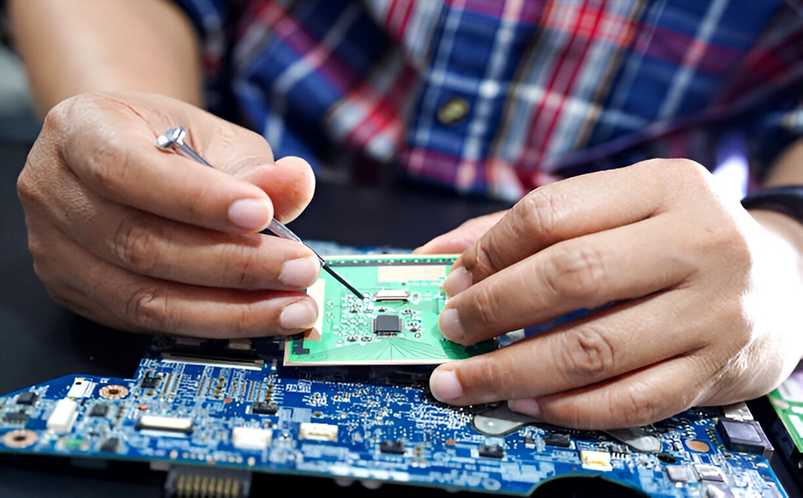
PCB repair is the process of restoring a defective printed circuit board by identifying and correcting damaged traces, solder joints, connectors, or failed components while preserving the board’s intended electrical and mechanical functionality.
Depending on the type of failure, PCB repair may involve:
- Visual inspection and fault identification
- Electrical testing and troubleshooting
- Component removal using appropriate desoldering techniques
- PCB pad or trace repair
- Cleaning and surface preparation
- Application of solder paste or flux where appropriate
- Component alignment and placement
- Soldering and rework
- Post-repair inspection
- Electrical and functional testing
A typical PCB repair workflow can be summarized as:
Inspection → Diagnosis → Component Removal → Surface Preparation → Replacement or Repair → Soldering → Inspection → Electrical Testing
The specific procedure depends on the PCB material, component package, board construction, defect type, and reliability requirements.
Common Problems During PCB Repair
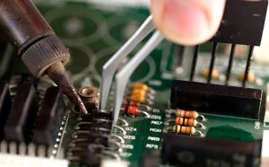
PCB repair requires controlled processes and trained technicians. Several problems can occur if appropriate procedures are not followed.
Electrical Overstress (EOS)
Electrical Overstress (EOS) occurs when an electronic component or circuit is exposed to electrical conditions beyond its specified limits, such as excessive voltage or current.
EOS can damage semiconductor devices, traces, connectors, and other circuit elements.
Improper testing equipment, incorrect power application, unsuitable component handling, or uncontrolled soldering and rework procedures can contribute to electrical overstress.
Technicians should therefore verify voltage and current limits before powering a repaired PCB.
Poor Electrical or Mechanical Connections
An unreliable solder joint can cause intermittent operation, increased resistance, open circuits, or complete component failure.
Potential causes include:
- Insufficient solder
- Excessive solder
- Poor surface preparation
- Contaminated pads
- Incorrect soldering temperature
- Insufficient heating
- Excessive component movement
- Incorrect component placement
Proper soldering parameters and inspection procedures are essential for achieving reliable connections.
Electrostatic Discharge (ESD) Damage
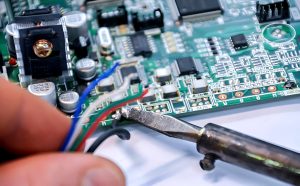
Electrostatic Discharge (ESD) is another major concern during PCB testing and repair.
Sensitive semiconductor devices can be damaged by an electrostatic event even when there is no immediately visible physical damage.
Therefore, PCB repair areas should use appropriate ESD control measures, including:
- ESD-safe workstations
- Grounded wrist straps
- ESD-safe tools
- Appropriate protective packaging
- Proper grounding and personnel procedures
ESD control is especially important when handling microcontrollers, memory devices, MOSFETs, sensors, RF components, and other sensitive semiconductor devices.
PCB Repair Dos
Following appropriate repair practices can reduce the risk of secondary damage and improve the reliability of repaired boards.
1. Preheat the PCB When Appropriate
Suddenly applying high heat to a localized area of a PCB can create thermal stress.
Controlled preheating can help reduce temperature gradients and thermal shock, particularly when performing rework on multilayer boards or assemblies containing moisture-sensitive materials.
During controlled rework, the PCB may be secured using an appropriate fixture to prevent unnecessary movement. A controlled thermal profile can also help reduce the risk of board warpage.
However, preheating should not be treated as a universal requirement for every repair. The appropriate temperature profile depends on the PCB construction, component specifications, solder alloy, rework equipment, and applicable process requirements.
For complex assemblies, technicians should follow the component and board manufacturer’s recommended thermal limits.
2. Follow Industry Standards and Repair Procedures
Professional PCB Repair should be performed according to applicable industry standards and documented work instructions.
Standards such as IPC workmanship and acceptance criteria can provide guidance for solder joints, component placement, conductor repair, and assembly quality.
Depending on the application, relevant requirements may include standards associated with:
- PCB acceptability
- Electronic assembly workmanship
- Component handling
- ESD control
- Soldering and rework
- Electrical testing
Following established standards helps ensure that repairs are evaluated consistently rather than relying only on visual judgment.
3. Inspect the PCB After Repair
Post-repair inspection is an essential step.
A repaired board should be visually inspected to verify:
- Component orientation
- Component placement
- Solder joint quality
- Pad integrity
- Trace condition
- Solder bridges
- Excess solder
- Flux residues
- Mechanical damage
For hidden solder joints, such as those underneath certain BGA packages, X-ray inspection may be appropriate when required by the component package and application.
Electrical testing should also be performed to confirm that the repaired circuit operates according to its intended specifications.
For high-reliability production environments, repair records and applicable quality documentation should be maintained. Where a Certificate of Conformance (CoC) is contractually or procedurally required, it should be issued according to the applicable quality system and customer requirements.
4. Use the Correct Amount of Solder
The amount of solder used during PCB repair must be carefully controlled.
Too little solder can produce an insufficient mechanical and electrical connection, while excessive solder can create solder bridges and unintended connections between adjacent pads.
The correct solder volume depends on factors such as:
- Pad geometry
- Component package
- Lead pitch
- Solder alloy
- Soldering method
- PCB surface finish
Technicians should use appropriate tools and process parameters rather than relying on excessive solder to compensate for poor alignment or insufficient heating.
5. Keep the PCB and Repair Area Clean
Surface contamination can interfere with solder wetting and electrical performance.
Before soldering, the repair area should be properly prepared and cleaned using a compatible process. After repair, flux residues and other contaminants should be removed when required by the flux chemistry, board design, and application.
Cleaning procedures must be compatible with the PCB materials, components, coatings, and labels.
PCB Repair Don’ts
Avoiding common repair mistakes is just as important as following the correct repair procedure.
1. Do Not Accidentally Move or Damage Adjacent Components
When removing or replacing a failed component, nearby components should be protected from mechanical and thermal damage.
Excessive force or uncontrolled desoldering can cause:
- Lifted pads
- Damaged traces
- Cracked components
- Disturbed solder joints
- Component displacement
- Delamination or other PCB damage
After completing the repair, inspect the surrounding area rather than checking only the repaired component.
2. Do Not Overheat the PCB
Excessive heat is one of the most common risks during PCB rework.
Overheating can damage:
- Semiconductor components
- Connectors
- Plastic housings
- Solder joints
- PCB laminates
- Solder mask
- Adhesive materials
Technicians should establish appropriate temperature limits based on the PCB assembly and component specifications.
For heat-sensitive components, appropriate thermal management techniques can be used to reduce unnecessary heat exposure.
3. Do Not Move Components While the Solder Is Molten
Component alignment is critical to achieving reliable solder joints.
Moving a component while the solder is still molten can result in:
- Misalignment
- Poor wetting
- Insufficient solder coverage
- Solder bridges
- Weak mechanical connections
Components should be positioned correctly before soldering and allowed to stabilize during the appropriate stages of the process.
4. Do Not Allow Untrained Personnel to Perform PCB Repair
PCB repair requires knowledge of electronics, soldering, component handling, ESD control, inspection, and testing.
Untrained personnel may unintentionally cause additional damage or create safety and quality problems.
Professional technicians should receive appropriate training before performing PCB rework, particularly when working with:
- High-density SMT assemblies
- BGA packages
- Fine-pitch components
- High-voltage circuits
- RF circuits
- High-reliability electronics
For critical products, repair personnel should also follow documented procedures and applicable certification or training requirements.
5. Do Not Skip Inspection and Testing
A PCB should never be considered successfully repaired simply because the replacement component has been soldered into place.
Post-repair inspection and testing are essential for verifying the effectiveness of the repair.
Depending on the application, testing may include:
- Visual inspection
- Continuity testing
- Resistance measurements
- Insulation testing
- Power-on testing
- Functional testing
- Automated optical inspection (AOI)
- X-ray inspection
- In-circuit testing (ICT)
- Other application-specific electrical tests
Testing requirements should be determined by the PCB design, product specifications, repair procedure, and applicable industry standards.
PCB Repair Best Practices for Reliable Results
Beyond the basic dos and don’ts, several additional practices can improve the quality and repeatability of PCB repair.
Diagnose the Root Cause Before Replacing Components
Replacing a visibly damaged component does not necessarily solve the underlying problem.
For example, a failed MOSFET may have been caused by:
- Excessive voltage
- Short circuit
- Incorrect gate drive
- Thermal stress
- Power supply instability
- Previous component failure
Technicians should investigate the root cause whenever practical. Otherwise, the replacement component may fail again after the PCB is returned to service.
Protect the PCB During Rework
The board should be properly supported during repair.
Large or flexible boards can experience mechanical stress when excessive force is applied to components. Appropriate fixtures can help stabilize the PCB and reduce bending during component removal and installation.
Use Appropriate Rework Equipment
The repair method should match the component and PCB structure.
Depending on the application, equipment may include:
- Temperature-controlled soldering stations
- Hot-air rework systems
- Preheating systems
- BGA rework equipment
- Microscopes
- ESD-safe tools
- Digital multimeters
- Oscilloscopes
- Programmers
- X-ray inspection equipment
Using the appropriate equipment improves process control and reduces the risk of secondary damage.
Record the Repair Process
For production and high-reliability applications, repair records can provide valuable traceability.
A repair record may include:
- PCB identification
- Failure description
- Root-cause analysis
- Replaced components
- Repair method
- Technician information
- Inspection results
- Electrical test results
- Final disposition
This information can help manufacturers identify recurring failure patterns and improve the original PCB Design or PCB Manufacturing process.
PCB Repair vs. PCB Replacement
Whether to repair or replace a PCB depends on the defect, board value, complexity, repairability, and reliability requirements.
| Factor | PCB Repair | PCB Replacement |
|---|---|---|
| Cost | Potentially lower for localized faults | May be higher for expensive or complex boards |
| Lead time | Can be fast for simple repairs | Depends on replacement availability |
| Suitable defects | Component failures, localized trace or solder issues | Severe structural damage or extensive failure |
| Traceability | Requires detailed repair records | Usually follows standard production records |
| Reliability | Depends heavily on repair quality | Depends on replacement board quality |
| Application | Useful for service and rework | Useful when repair is impractical |
Repair is not always the appropriate solution. Severe delamination, extensive burning, widespread corrosion, major mechanical damage, or damage to critical internal structures may make replacement more practical.
The decision should therefore be based on engineering evaluation rather than cost alone.
How PCB Design Can Reduce Future Repair Problems
Good PCB Design can make future troubleshooting and repair significantly easier.
Engineers should consider:
- Adequate component spacing
- Accessible test points
- Clear reference designators
- Proper thermal management
- Appropriate component ratings
- ESD protection
- Overvoltage and overcurrent protection
- Clearly documented circuit functions
- Suitable PCB materials
- Manufacturable component footprints
Design for manufacturability (DFM) and design for testability (DFT) can also help reduce production defects and simplify troubleshooting.
A repair-friendly PCB design can reduce service time and make component-level diagnosis more efficient.
The Role of PCB Manufacturing in Repair Reliability
PCB repair quality is closely related to the quality of the original manufacturing process.
Manufacturing defects such as poor solder joints, insufficient plating, contamination, incorrect component placement, or damaged traces can become recurring failure sources.
Therefore, reliable PCB Manufacturing should include appropriate inspection and testing throughout production.
Depending on the product, manufacturers may use:
- Automated Optical Inspection (AOI)
- X-ray inspection
- In-Circuit Testing (ICT)
- Flying-probe testing
- Electrical continuity testing
- Functional testing
- Dimensional inspection
- Solderability evaluation
At Kingda, PCB design, manufacturing, assembly, inspection, and repair considerations can be evaluated as interconnected parts of the electronics production process. This integrated approach helps identify potential manufacturing issues earlier and supports more reliable PCB products.
Conclusion
PCB Repair is a practical way to restore circuit-board functionality when the underlying damage is localized and the board remains structurally suitable for rework. However, successful repair requires more than simply replacing a failed component.
Technicians should first diagnose the root cause, protect the PCB against ESD and excessive thermal stress, use appropriate rework equipment, control soldering parameters, and carefully inspect the repaired area.
The most important PCB repair dos include appropriate preheating when required, following applicable industry standards, maintaining adequate solder volume, protecting adjacent components, and performing post-repair inspection and electrical testing.
At the same time, technicians should avoid overheating the board, moving components while solder is molten, using excessive solder, allowing untrained personnel to perform complex repairs, or skipping final inspection and testing.
From initial PCB Design through PCB Manufacturing, assembly, testing, and field service, a systematic engineering approach can improve PCB reliability and reduce the risk of recurring failures. For professional electronics manufacturers, establishing clear repair procedures and maintaining accurate repair records are also important for long-term quality improvement.