Bare Board Testing: PCB Design, PCB Manufacturing & Open/Short Circuit Testing
In modern electronics manufacturing, especially in PCB Manufacturing, ensuring that a circuit board is electrically and physically sound before component assembly is essential. One of the fundamental quality-control processes used for this purpose is bare board testing (BBT), also commonly referred to as PCB open and short testing.
Unlike PCBA testing, bare board testing is performed before electronic components are mounted on the PCB. Its primary purpose is to verify that the manufactured circuit board accurately matches the intended PCB Design and that all conductive paths, isolated circuits, vias, pads, and other critical features meet the required electrical specifications.
A defective PCB that passes into the assembly stage can cause additional labor, component loss, rework, and troubleshooting costs. For this reason, manufacturers such as Kingda use systematic bare board inspection and electrical testing to identify manufacturing defects as early as possible.
This article explains what bare board testing is, why it matters, how PCB open and short testing is performed, and which inspection and quality-control methods should be considered.
What Is Bare Board Testing?
Bare board testing is the process of inspecting and electrically testing a manufactured PCB before components are assembled onto it.
The process generally focuses on verifying:
- Electrical continuity between designated conductive points
- Electrical isolation between circuits that should remain separate
- PCB traces and connections
- Vias and plated through-holes
- Pads and other conductive features
- Layer-to-layer interconnections
- Selected controlled-impedance structures
- Manufacturing defects that could affect electrical performance
The fundamental objective is simple: make sure the bare PCB is manufactured according to the design before it becomes a populated PCBA.
Why Is Bare Board Testing Important?
Bare board testing provides several important advantages throughout the PCB production process.
1. Early Defect Detection
Detecting defects during the early stages of production can significantly reduce downstream costs.
Common defects include:
- Open circuits
- Short circuits
- Missing or incomplete traces
- Incorrect connections
- Plating defects
- Via-related failures
- Copper-to-copper shorts
- Manufacturing deviations
If these defects are discovered after component assembly, troubleshooting becomes considerably more complicated. Components may need to be removed, boards may require rework, and valuable production time can be lost.
By performing PCB open and short testing before assembly, manufacturers can prevent defective bare boards from entering the SMT or through-hole assembly process.
2. Verification of PCB Design Integrity
Bare board testing also helps verify that the manufactured PCB corresponds to the intended design data.
During PCB Design, engineers define the electrical relationships between nets, traces, vias, pads, and other conductive structures. During manufacturing, these design requirements must be accurately transferred to the physical board.
Electrical testing helps confirm that the manufactured board maintains those intended connections and isolation relationships.
3. Compliance With Manufacturing Requirements
PCB manufacturers must meet applicable customer specifications, fabrication requirements, and industry standards.
Depending on the application, requirements may include:
- IPC workmanship and acceptability criteria
- Customer-specific electrical test requirements
- Controlled impedance requirements
- Minimum insulation resistance
- High-voltage or dielectric withstand requirements
- Dimensional and mechanical specifications
The exact requirements vary according to the PCB type and end application.
4. Cost Reduction
Testing a bare PCB is generally more economical than discovering a defect after components have been installed.
Consider a board that contains a hidden short circuit. If the defect is detected before assembly, the manufacturer can isolate the defective board. If it reaches SMT assembly, additional components, soldering processes, inspection, and troubleshooting may already have been performed.
Therefore, bare board testing acts as an important quality gate between PCB fabrication and PCB assembly.
How to Prepare for Bare Board Testing
Proper preparation is critical for obtaining reliable test results.
1. Review the PCB Design Files
The first step is to collect and verify the manufacturing data.
Depending on the production workflow, this may include:
- Gerber files
- ODB++ or other manufacturing data
- Drill files
- Netlist information
- Stackup information
- Impedance requirements
- Test-point information
- Customer specifications
The netlist is particularly important for electrical testing because it defines which points should be electrically connected and which points should remain isolated.
The test system can compare the actual PCB against these design relationships to identify unexpected opens or shorts.
2. Prepare the Test Equipment
The appropriate testing system should be selected according to the PCB design, production volume, board complexity, and required test coverage.
Common systems include:
- Flying probe testers
- Fixture-based or bed-of-nails testers
- Dedicated electrical test systems
The equipment should be properly configured before testing begins. Test parameters, probes, fixtures, software data, and board identification should all be verified.
Regular equipment calibration and maintenance are also important for maintaining measurement accuracy.
3. Perform a Preliminary Visual Inspection
Before electrical testing, the bare PCB should be visually inspected for obvious manufacturing abnormalities.
Inspectors may look for:
- Layer misalignment
- Damaged edges
- Copper defects
- Scratches
- Contamination
- Abnormal solder mask
- Missing or damaged pads
- Plating abnormalities
- Warpage or deformation
Visual inspection does not replace electrical testing, but it can identify physical defects that may affect subsequent testing or assembly.
How Is PCB Open and Short Testing Performed?
The primary purpose of electrical bare board testing is to verify continuity and isolation.
Two major testing approaches are commonly used: flying probe testing and fixture-based testing.
Flying Probe Testing
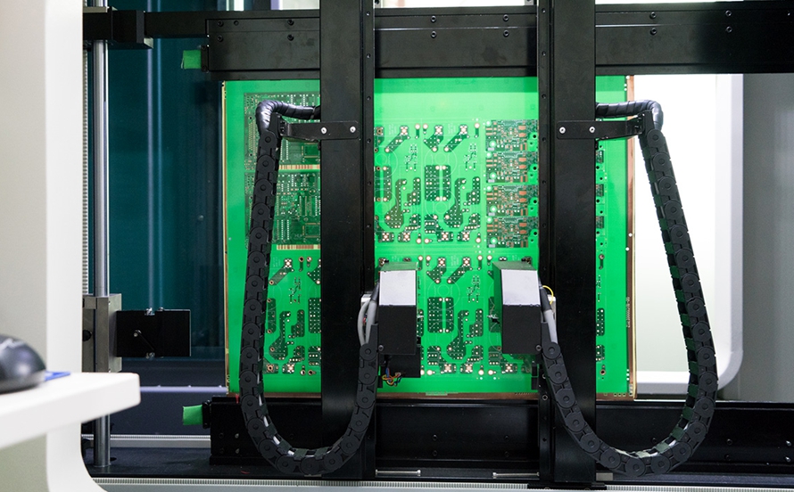
Flying probe testing uses movable probes controlled by a test program.
Unlike a dedicated fixture, a flying probe tester does not normally require a permanent test fixture designed specifically for one PCB. The probes move automatically to predetermined test locations based on the PCB’s test data.
The general process is:
- Load the PCB test data into the testing system.
- Position the bare PCB on the tester.
- Establish the required reference and test points.
- Move the probes to designated conductive locations.
- Measure electrical continuity between points that should be connected.
- Measure isolation between points that should remain electrically separate.
- Compare the measured results with the expected netlist and test limits.
- Record and classify any failures.
Flying probe testing is particularly useful for prototypes, new product introductions, and low-to-medium-volume production because it provides flexibility without requiring a dedicated fixture for every board design.
Fixture-Based Testing
Fixture-based electrical testing, often called bed-of-nails testing, uses a customized fixture containing numerous spring-loaded probes.
The fixture establishes contact with predetermined test points on the PCB and allows multiple electrical measurements to be performed rapidly.
This approach can provide high throughput for stable, high-volume production. However, developing and manufacturing the fixture introduces additional setup time and tooling costs.
Therefore, the choice between flying probe and fixture-based testing depends on production volume, PCB complexity, product lifecycle, and cost considerations.
Key Electrical Tests in Bare Board Testing
1. Continuity Testing
Continuity testing verifies that electrically connected points actually have a conductive path between them.
For example, the test can verify connections involving:
- Pads
- Traces
- Vias
- Through-holes
- Internal copper layers
- Connector contacts
An unexpected open circuit indicates that the intended conductive path is incomplete or has excessive electrical resistance beyond the defined test limit.
Possible causes include broken traces, insufficient copper, defective vias, drilling problems, or plating failures.
2. Isolation Testing
Isolation testing verifies that circuits that should remain electrically separated do not have an unintended conductive path between them.
This is essential for detecting PCB short circuits.
Potential causes of shorts include:
- Copper bridges
- Over-etched structures
- Insufficient spacing
- Plating defects
- Contamination
- Manufacturing residues
- Design-related clearance problems
Isolation testing is especially important for dense PCB designs with fine-pitch routing and small conductor spacing.
3. Impedance Testing
For high-speed PCB designs, controlled impedance can be an important electrical requirement.
Impedance testing verifies whether designated transmission-line structures fall within the specified impedance range.
Controlled impedance is particularly relevant to circuits carrying high-speed signals such as:
- USB
- PCIe
- Ethernet
- DDR memory
- RF signals
- High-speed serial interfaces
Impedance testing is different from basic open/short testing because it evaluates transmission-line characteristics rather than simply determining whether two points are electrically connected.
Analyzing Bare Board Test Results
After electrical testing is complete, the results should be reviewed systematically.
A typical test report may include:
- Board identification
- Test date and time
- Test program version
- Number of nets tested
- Continuity results
- Isolation results
- Impedance results where applicable
- Failed locations
- Failure classifications
- Repair or disposition information
Modern testing systems can automatically record failure locations and provide diagnostic information that helps engineers determine the probable source of a defect.
Traceability is particularly important for production environments because test records can later be used for quality analysis, process improvement, and customer documentation.
Defect Handling and Retesting
Finding a defective PCB is only the beginning. The next step is determining whether the board can be repaired or should be rejected.
1. Defect Analysis and Repair
The appropriate response depends on the defect type, PCB construction, customer requirements, and applicable manufacturing procedures.
Potential corrective actions may include:
- Repairing an approved trace defect
- Reworking a manufacturing defect when technically permissible
- Correcting localized conductive issues
- Reprocessing the board under an approved procedure
- Scrapping the PCB when repair is not acceptable
Not every bare-board defect should be repaired. High-reliability applications may have strict limitations on repair or rework.
Any repair should be performed by qualified personnel using controlled procedures to prevent additional damage to traces, pads, dielectric materials, or plated holes.
2. Retesting
A repaired PCB should be retested according to the applicable procedure.
The purpose of retesting is to verify that:
- The original defect has been eliminated.
- No new electrical defect was introduced.
- Continuity requirements are satisfied.
- Isolation requirements are satisfied.
- Applicable electrical specifications are met.
This makes retesting a critical part of the PCB open and short testing process.
Final Inspection and Quality Control
After electrical testing and any approved corrective actions, the PCB should undergo final quality verification before being released for assembly.
1. Visual Inspection
A final visual inspection can identify remaining physical abnormalities that may not be detected by electrical testing.
Inspectors may verify:
- Surface condition
- Solder mask coverage
- Silkscreen markings
- Pad condition
- Hole quality
- Board edges
- Surface contamination
- Mechanical damage
- Dimensional conformity
2. Automated Optical Inspection (AOI)
AOI systems use cameras and image-processing software to inspect PCB features.
Depending on the system and manufacturing stage, AOI can help identify issues such as:
- Missing or damaged features
- Pattern abnormalities
- Registration errors
- Trace-related defects
- Pad abnormalities
- Surface defects
AOI and electrical testing serve different purposes and are often complementary rather than interchangeable.
3. Final Test Documentation
Once the inspection and testing process has been completed, the manufacturer should maintain appropriate test records.
A final quality report may contain:
- Test results
- Inspection results
- Defect information
- Corrective actions
- Retest results
- Final disposition
- Traceability information
For manufacturers such as Kingda, systematic documentation can support production traceability and continuous process improvement.
Bare Board Testing Best Practices
Several practices can improve the reliability and efficiency of bare board testing.
Calibrate Testing Equipment Regularly
Testing equipment should be maintained and calibrated according to the manufacturer’s recommendations and the applicable quality system.
A properly maintained tester helps reduce measurement uncertainty and prevents equipment-related false failures.
Use Correct Test Data
Incorrect or outdated test data can produce misleading results. The test program should correspond to the correct PCB revision and manufacturing data.
This is particularly important when engineers make PCB revisions during product development.
Train Testing Personnel
Operators and technicians should understand:
- Test procedures
- Equipment operation
- Safety requirements
- Failure classification
- Retest procedures
- Traceability requirements
Proper training reduces operator-related errors and improves consistency.
Choose the Appropriate Test Method
There is no single electrical test method that is ideal for every PCB.
Flying probe testing may be appropriate for prototypes and lower-volume production, while fixture-based testing can be advantageous for high-volume manufacturing.
The selection should consider:
- Production volume
- Board complexity
- Test coverage
- Fixture cost
- Development schedule
- Product lifecycle
- Required throughput
Maintain Complete Test Records
Test results should be linked to appropriate board or production identifiers whenever traceability is required.
Historical data can help manufacturers identify recurring defects, monitor process stability, and improve future PCB Manufacturing processes.
PCB Design Considerations for Better Bare Board Testing
Bare board testing should not be considered only a manufacturing activity. Good PCB Design practices can make electrical testing easier and more reliable.
Designers should consider:
- Accessible test points
- Appropriate spacing
- Clear net identification
- Adequate conductor-to-conductor clearance
- Controlled impedance structures where required
- Manufacturability requirements
- Test accessibility
- Board complexity
- Revision control
Design for Testability (DFT) can help reduce test difficulty and improve fault coverage.
For example, strategically placed test points can provide easier probe access, while appropriate spacing can reduce the possibility of manufacturing-related shorts and simplify fixture design.
Flying Probe vs. Fixture-Based Testing
| Feature | Flying Probe Testing | Fixture-Based Testing |
|---|---|---|
| Fixture requirement | Usually no dedicated fixture | Dedicated fixture normally required |
| Setup cost | Generally lower | Higher due to fixture |
| Flexibility | High | Lower after fixture creation |
| Prototype suitability | Excellent | Less suitable |
| High-volume suitability | Good, depending on cycle time | Excellent |
| Test speed | Generally slower | Generally faster |
| PCB changeover | Relatively easy | May require fixture modification |
| Best use | Prototypes and varied production | Stable high-volume production |
The appropriate solution depends on the specific production requirements rather than simply choosing the fastest testing technology.
Bare Board Testing vs. PCBA Testing
It is important to distinguish bare board testing from PCBA testing.
| Bare Board Testing | PCBA Testing |
|---|---|
| Performed before component assembly | Performed after components are installed |
| Focuses on PCB fabrication quality | Evaluates assembled electronic functionality |
| Checks opens and shorts | May include functional and in-circuit testing |
| Verifies PCB interconnections | Tests components and assembled circuits |
| Helps prevent defective boards from reaching assembly | Helps verify final assembly performance |
Both processes are important, but they address different stages of the manufacturing process.
Conclusion
Bare board testing is a critical quality-control step between PCB fabrication and component assembly. Through systematic PCB open and short testing, manufacturers can identify continuity failures, unintended shorts, defective interconnections, and other electrical problems before additional manufacturing costs are incurred.
A comprehensive testing strategy typically combines design-data verification, visual inspection, electrical testing, defect analysis, retesting, and final documentation. The selection of flying probe or fixture-based testing should be based on production volume, board complexity, test coverage, and cost requirements.
For engineers, procurement teams, and electronics manufacturers, integrating testability into PCB Design and maintaining strict controls throughout PCB Manufacturing can improve production efficiency, reduce rework, and support consistent PCB quality.
Kingda can support PCB projects with manufacturing-oriented engineering, electrical testing, inspection, and quality-control processes designed to help ensure that bare boards meet the required design and production specifications before assembly.