Circuit Board Diagram: PCB Design, PCB Manufacturing & Schematic Guide
In modern electronics, the printed circuit board (PCB) is an essential part of almost every electronic product. It provides both the mechanical platform and electrical interconnection system required to mount and connect electronic components. From simple consumer devices to advanced industrial, automotive, medical, telecommunications, and aerospace systems, PCBs play a fundamental role in modern electronics.
Since the development of PCB technology, the industry’s focus on miniaturization, higher efficiency, faster signal transmission, and improved reliability has continued to drive advances in PCB Design, materials, fabrication, and assembly.
A PCB typically consists of conductive copper patterns formed on and between insulating dielectric materials. Components such as resistors, capacitors, diodes, transistors, integrated circuits, and connectors are mounted on the board and electrically interconnected through traces, vias, and other conductive structures.
PCBs can be manufactured in many configurations, including single-sided, double-sided, and multilayer boards, as well as rigid, flexible, and rigid-flex constructions.
However, before a PCB can be manufactured, engineers need a clear representation of how the electronic circuit is supposed to function. This is where a circuit board diagram, particularly a schematic diagram, becomes essential.
Understanding circuit diagrams helps engineers design, manufacture, test, troubleshoot, and maintain electronic systems more effectively.
What Is a Circuit Board Diagram?
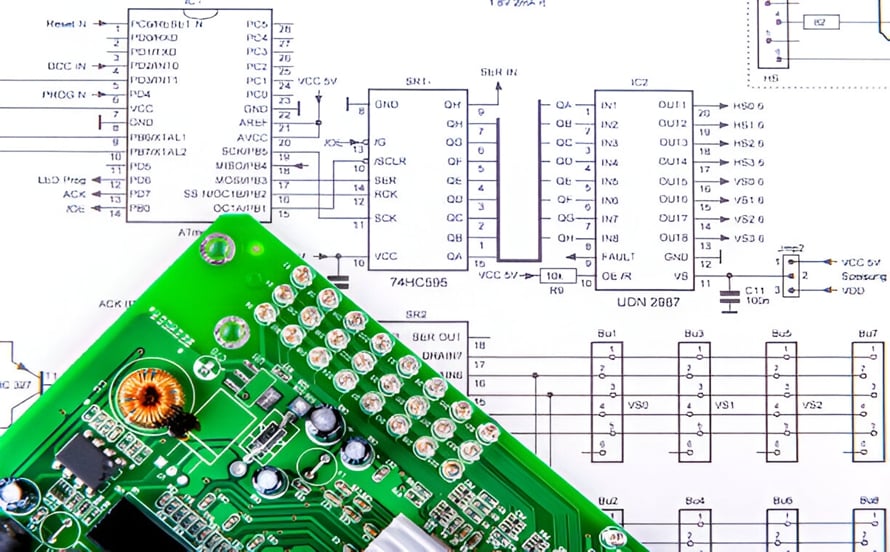
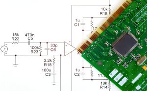
A circuit board diagram is a graphical representation of an electronic circuit and its electrical relationships.
In professional electronics engineering, the term usually refers to a schematic diagram, which uses standardized symbols and connection lines to describe how electronic components are electrically connected.
A schematic may represent components such as:
- Resistors
- Capacitors
- Inductors
- Diodes
- Transistors
- Integrated circuits
- Connectors
- Switches
- Sensors
- Power sources
The schematic focuses primarily on electrical connectivity and circuit functionality, rather than showing the physical position of components on the manufactured PCB.
This distinction is important.
A schematic shows what is connected to what, while a PCB layout shows where the components and physical copper structures are located.
Both are essential parts of the overall PCB Design process.
Circuit Diagram vs. PCB Layout
These two concepts are sometimes confused, but they serve different purposes.
| Feature | Circuit Schematic | PCB Layout |
|---|---|---|
| Main purpose | Defines electrical relationships | Defines physical implementation |
| Components | Represented by symbols | Represented by footprints |
| Connections | Nets and schematic wires | Copper traces, vias, and planes |
| Physical location | Generally not important | Critical |
| Main use | Circuit design and analysis | PCB fabrication |
| Output | Schematic/netlist | Gerber, drill, and manufacturing data |
The schematic is normally created first. The design information is then transferred into the PCB layout environment, where engineers place components and route physical connections.
Designing a PCB From a Circuit Board Diagram
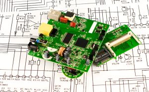
The schematic is one of the most important starting points in PCB Design.
A typical design workflow includes several major stages.
1. Schematic Design
Engineers first create the circuit schematic to represent the intended electrical architecture.
The schematic should clearly define:
- Components
- Component values
- Net connections
- Power rails
- Ground connections
- Connectors
- Signal paths
- Interfaces
- Designators
- Electrical relationships
A well-organized schematic makes later PCB layout, debugging, documentation, and manufacturing much easier.
2. Component Selection and Footprints
After the schematic has been completed, each component must be associated with an appropriate PCB footprint.
The footprint defines the physical land pattern required for assembly.
Important considerations include:
- Package type
- Pad dimensions
- Pin spacing
- Component height
- Thermal requirements
- Assembly technology
- Manufacturer recommendations
An incorrect footprint can result in serious assembly or electrical problems even when the schematic itself is correct.
3. Component Placement
The selected footprints are then placed on the PCB.
Component placement should consider:
- Functional relationships
- Signal-path length
- Power distribution
- Thermal management
- Mechanical constraints
- Connector locations
- High-speed interfaces
- EMI considerations
- Manufacturing accessibility
Components that exchange high-speed signals should generally be positioned to minimize unnecessary routing distance.
Similarly, decoupling capacitors should normally be located close to the relevant IC power pins to reduce parasitic inductance.
4. PCB Routing
Once the placement has been established, engineers route the connections between components.
PCB routing involves creating physical copper traces based on the electrical nets defined by the schematic.
Routing requirements may include:
- Trace width
- Trace spacing
- Differential-pair geometry
- Controlled impedance
- Via placement
- Return-current paths
- Length matching
- Power routing
- Ground-plane continuity
For high-speed designs, routing must consider not only the signal path but also the associated return-current path.
5. Design Rule Check (DRC)
Before manufacturing, the PCB layout should undergo a Design Rule Check (DRC).
DRC verifies whether the layout complies with predefined design constraints.
Typical checks include:
- Minimum trace width
- Minimum clearance
- Via dimensions
- Hole sizes
- Copper-to-edge clearance
- Solder mask clearance
- Unconnected nets
- Manufacturing constraints
- Component spacing
DRC is an important step, but it does not replace engineering review or electrical simulation.
6. Generate Manufacturing Files
After the PCB layout has been finalized, manufacturing data is generated.
Depending on the manufacturing workflow, this may include:
- Gerber files
- NC drill files
- Pick-and-place files
- Fabrication drawings
- Assembly drawings
- Bill of materials (BOM)
- Stackup documentation
- Impedance specifications
Gerber files are commonly used to communicate PCB fabrication layer information to the manufacturer.
The exact data package depends on whether the project involves bare PCB fabrication, PCB assembly, or both.
How Is a PCB Manufactured From a Circuit Board Design?
Once the design has been finalized and manufacturing data has been verified, PCB Manufacturing begins.
The exact process depends on the board type, material, layer count, copper thickness, surface finish, and other specifications.
1. Material Preparation and Lamination
Common PCB materials include FR-4 and other specialized dielectric systems.
For multilayer PCBs, copper foils, cores, and prepreg materials are combined into a defined stackup.
The layers are laminated under controlled temperature and pressure to create a mechanically stable multilayer structure.
2. Imaging and Copper Etching
The required circuit pattern is transferred onto the copper surface through an imaging process.
Unwanted copper is then removed during etching, leaving the desired conductive pattern.
The goal is to reproduce the circuit geometry defined by the PCB manufacturing data.
3. Drilling
Mechanical or laser drilling creates holes required for:
- Through-hole components
- Plated through-holes
- Vias
- Mounting holes
- Other mechanical features
The drill data is generated from the PCB design and manufacturing files.
4. Plating and Layer Interconnection
For multilayer boards, plated holes and vias provide electrical connections between different copper layers.
A conductive copper layer is deposited inside appropriate drilled holes, creating reliable interlayer electrical connections.
The plating process also contributes to the final copper thickness and current-carrying capability of relevant features.
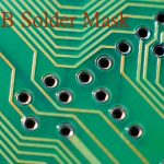
5. Solder Mask Application
A protective solder mask is applied to the PCB surface.
It covers most exposed copper while leaving designated pads and other required areas open.
Solder mask helps:
- Protect copper
- Reduce oxidation
- Prevent solder bridges
- Provide electrical insulation
- Improve surface durability
Green is the most familiar solder mask color, although other colors are also available.
6. Surface Finish
The exposed copper pads may receive a surface finish to improve solderability and protect the copper.
Common surface finishes include:
- HASL
- Lead-free HASL
- ENIG
- OSP
- Immersion tin
- Immersion silver
- ENEPIG
The appropriate finish depends on the component pitch, assembly process, reliability requirements, storage conditions, and cost considerations.
7. Silkscreen Printing
The silkscreen layer provides useful visual information such as:
- Reference designators
- Component labels
- Polarity indicators
- Logos
- Assembly instructions
- Warning symbols
Silkscreen improves assembly, inspection, maintenance, and troubleshooting.
8. Final Inspection and Testing
The completed PCB is inspected and tested before being released for assembly or shipment.
Depending on the product requirements, quality-control processes may include:
- Visual inspection
- Automated optical inspection (AOI)
- Electrical continuity testing
- Open/short testing
- Dimensional inspection
- Microsection analysis
- Controlled impedance testing
- Other application-specific tests
The objective is to verify that the manufactured board conforms to the approved design and manufacturing specifications.
Types of PCBs Used in Circuit Board Design
PCB structures vary according to layer count, mechanical construction, flexibility, material, and application.
1. Single-Sided PCB
A single-sided PCB contains conductive copper primarily on one side of the insulating substrate.
Because of its relatively simple construction and low manufacturing cost, it is commonly used in simpler electronic products where routing density is limited.
Typical applications include:
- Basic consumer electronics
- Simple control circuits
- Low-cost electronic products
- Basic power and interface boards
2. Double-Sided PCB
A double-sided PCB has conductive copper layers on both sides of the dielectric substrate.
Vias and plated through-holes can connect the two copper layers, providing greater routing flexibility than a single-sided board.
Double-sided PCBs are widely used in:
- Home appliances
- Industrial controls
- Consumer electronics
- Power electronics
- Communication equipment
3. Multilayer PCB
A multilayer PCB contains multiple conductive copper layers separated by dielectric materials.
Multilayer boards can provide:
- Greater routing capacity
- Dedicated ground planes
- Power planes
- Better signal isolation
- Controlled impedance
- Higher circuit density
They are widely used in computers, smartphones, networking equipment, automotive electronics, medical devices, and other complex systems.
4. Rigid PCB
A rigid PCB uses a mechanically stable substrate and is not intended to be repeatedly bent during normal operation.
FR-4 is one of the most widely used rigid PCB materials.
Rigid PCBs are found in products such as:
- Computers
- Industrial controllers
- Consumer electronics
- Automotive control modules
- Test equipment
5. Flexible PCB
A flexible PCB uses flexible dielectric materials and can bend or conform to the mechanical structure of a product.
Flexible circuits are particularly useful when:
- Space is limited
- Weight must be reduced
- Components or modules move relative to each other
- Conventional wiring would be difficult to route
Typical applications include cameras, wearable electronics, displays, and compact consumer devices.
6. Rigid-Flex PCB
A rigid-flex PCB combines rigid board sections with flexible circuit sections within a single interconnected structure.
This architecture can reduce the need for separate connectors and cables while providing both mechanical support and flexible routing.
Rigid-flex technology is used in applications including:
- Medical electronics
- Aerospace systems
- Defense electronics
- High-density industrial equipment
- Advanced consumer electronics
Applications of PCBs
PCBs designed from circuit schematics are used across virtually every major electronics industry.
Consumer Electronics
Smartphones, laptops, televisions, appliances, gaming equipment, and other consumer products use PCBs to interconnect processors, memory, displays, sensors, power systems, and communication interfaces.
Industrial Electronics
Industrial control systems use PCBs in:
- PLCs
- Motor controllers
- Automation systems
- Measurement equipment
- Human-machine interfaces
- Power-control systems
These boards often require high reliability and stable operation under demanding environmental conditions.
Automotive Electronics
Modern vehicles contain numerous PCBs for:
- Instrument clusters
- Infotainment
- Navigation
- Engine control
- ADAS
- Lighting
- Body control
- Airbag systems
- Battery management
Automotive PCBs often require enhanced thermal, mechanical, and environmental reliability.
Medical Electronics
PCBs are essential in medical equipment such as:
- Patient monitoring systems
- Diagnostic equipment
- Imaging systems
- Laboratory instruments
- Portable medical devices
Medical electronics generally place strong emphasis on reliability, traceability, and manufacturing quality.
Telecommunications
Routers, switches, wireless equipment, modems, optical communication systems, and network infrastructure depend on sophisticated PCBs to process and transmit electrical signals.
High-speed telecommunications boards often require controlled impedance, careful return-path design, low-loss materials, and strong EMI management.
Aerospace and Defense
Aerospace and defense electronics can require high-performance PCBs designed for demanding electrical, mechanical, thermal, and environmental conditions.
Applications may include:
- Communication systems
- Navigation systems
- Radar
- Avionics
- Control systems
- Electronic instrumentation
Why Circuit Board Diagrams Matter in PCB Manufacturing
A well-developed circuit diagram provides the foundation for successful PCB development.
It helps connect the different stages of the electronics production process:
Circuit Concept → Schematic → PCB Layout → DRC → Manufacturing Data → PCB Fabrication → Assembly → Testing
Errors introduced at the schematic stage can propagate into the PCB layout and eventually into manufacturing.
For this reason, engineers should verify the schematic before beginning detailed layout work.
Important checks include:
- Correct component values
- Correct component symbols
- Correct pin assignments
- Correct power connections
- Correct net names
- Proper grounding
- Appropriate signal connections
- Complete documentation
A robust schematic-to-layout workflow reduces the risk of design errors and simplifies later troubleshooting.
Best Practices for Circuit Board Diagram Design
Keep the Schematic Organized
Group related circuits together and arrange signal flow logically.
For example, a complex design may be divided into:
- Power supply
- Microcontroller
- Memory
- Analog circuitry
- Communication interfaces
- Sensors
- Output circuitry
This makes the schematic easier to understand and review.
Use Consistent Naming
Net names, component references, connectors, and functional blocks should follow a consistent naming convention.
Good naming makes debugging and design review considerably easier.
Separate Power and Signal Functions Clearly
Power distribution should be easy to identify.
Clearly defined power rails and ground connections help prevent accidental omissions and make PCB layout easier.
Verify Component Pin Assignments
Incorrect pin mapping is one of the most serious schematic-to-PCB errors.
Before finalizing the design, engineers should verify critical components against the manufacturer’s datasheet and recommended footprint.
Perform ERC and DRC
In addition to PCB DRC, schematic tools can perform Electrical Rule Check (ERC).
ERC can identify potential issues such as:
- Unconnected pins
- Conflicting pin types
- Missing power connections
- Suspicious electrical connections
Using both ERC and DRC creates a stronger verification workflow.
Conclusion
A circuit board diagram provides the logical foundation for developing an electronic product. While the schematic primarily describes electrical relationships, the PCB layout translates those relationships into physical components, traces, vias, copper planes, and other structures.
A successful PCB development process therefore requires close coordination between schematic design, component selection, placement, routing, verification, manufacturing-data generation, and fabrication.
Understanding the difference between a schematic and a physical PCB layout is especially important for engineers who work across PCB Design and PCB Manufacturing. A well-structured schematic can simplify layout, improve design review, reduce manufacturing errors, and make troubleshooting more efficient.
From single-sided and double-sided boards to advanced multilayer, flexible, and rigid-flex structures, Kingda can support PCB projects by combining design-oriented engineering considerations with manufacturing expertise. By establishing clear design data and manufacturing requirements from the beginning, customers can develop reliable PCBs that meet their electrical, mechanical, and application-specific requirements.