PCB Solder Mask: PCB Design, PCB Manufacturing & Solder Mask Materials
The electronics industry is evolving rapidly, and printed circuit boards (PCBs) are no exception. As demand continues to grow for smaller, faster, and more efficient electronic devices, the PCB industry is constantly advancing in materials, fabrication technologies, assembly processes, and quality-control methods.
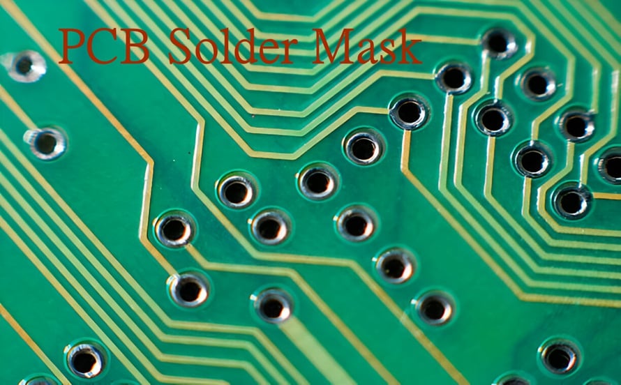
Modern PCB development focuses not only on electrical performance but also on manufacturability, reliability, thermal stability, and cost efficiency. One of the most important processes in PCB Manufacturing is applying the solder mask, the protective coating that covers most of the PCB surface and often gives the board its familiar green appearance.
Although green is the most recognizable solder mask color, manufacturers can use different solder mask materials and processes depending on the requirements of the application. The solder mask must provide reliable insulation and protection while remaining stable through PCB fabrication, soldering, assembly, and long-term operation.
This article explains what PCB solder mask is, why it is important, the major solder mask types, and how Liquid Photoimageable (LPI) solder mask and dry-film solder mask are applied during PCB manufacturing.
What Is PCB Solder Mask?
PCB solder mask, also called solder resist or solder resist mask, is a protective insulating layer applied over selected areas of a printed circuit board.
Its primary purpose is to prevent solder from unintentionally flowing onto areas where it is not required during PCB assembly. By covering exposed copper traces while leaving appropriate pads and other designated areas open, solder mask helps reduce the risk of solder bridges and accidental short circuits.
Solder mask also provides several other functions:
- Protects copper traces against oxidation
- Reduces exposure to moisture and environmental contaminants
- Helps prevent accidental solder bridging
- Provides electrical insulation between adjacent conductive features
- Improves PCB surface durability
- Helps protect traces from mechanical and chemical damage
- Provides visual contrast for inspection and assembly
The solder mask does not normally cover solderable pads, component terminals, or other areas that need to remain exposed for electrical or mechanical connections.
Because a PCB may experience repeated thermal cycles during fabrication and assembly, the selected PCB solder mask material must provide suitable thermal resistance, adhesion, chemical resistance, and dimensional stability.
Why Is Solder Mask Important in PCB Manufacturing?
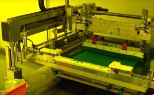
Solder mask is not simply a cosmetic coating. It is an important functional layer in PCB Manufacturing.
1. Preventing Solder Bridges
During reflow soldering or wave soldering, molten solder needs to remain confined to the intended solderable areas.
Solder mask separates neighboring copper features and reduces the possibility of solder flowing between them.
This is particularly important for fine-pitch components where the distance between adjacent pads can be very small.
2. Protecting Copper Traces
Exposed copper can oxidize when exposed to air, moisture, and other environmental factors.
Solder mask covers most of the copper circuitry and provides an additional protective barrier, helping maintain the long-term reliability of the PCB.
3. Providing Electrical Insulation
Solder mask creates an insulating layer between conductive features.
This can help reduce the possibility of accidental electrical contact between closely spaced traces, although the PCB’s underlying dielectric structure and design clearances remain the primary determinants of electrical insulation.
4. Improving PCB Reliability
A properly selected solder mask can help protect the PCB against:
- Moisture
- Dust
- Chemicals
- Mechanical abrasion
- Soldering heat
- Environmental contamination
For demanding applications, solder mask material selection should be based on the actual operating environment rather than simply choosing a standard material.
NSMD and SMD Pad Definitions
Solder-mask opening design is particularly important around component pads.
Two common pad definitions are Non-Solder Mask Defined (NSMD) and Solder Mask Defined (SMD).
Non-Solder Mask Defined (NSMD)
In an NSMD pad, the solder mask opening is larger than the copper pad, so the solder mask does not define the final pad boundary.
The copper pad is therefore exposed around its perimeter.
NSMD pads are commonly used in many PCB designs because they provide a larger exposed solderable area and can offer favorable solder-joint geometry.
Solder Mask Defined (SMD)
In an SMD pad, the solder mask opening is smaller than the copper pad, meaning that the solder mask overlaps the edge of the copper feature.
The solder mask therefore helps define the effective solderable area.
SMD pads can be useful in specific applications where mechanical strength, pad geometry, or component requirements make them appropriate.
The choice between NSMD and SMD should be based on component-package recommendations, PCB fabrication capabilities, pad geometry, and assembly requirements.
What Are the Main Types of PCB Solder Mask?
There are several solder mask technologies available for PCB production. Two important approaches are dry-film solder mask and Liquid Photoimageable solder mask (LPI).
The appropriate technology depends on PCB design requirements, production volume, surface geometry, feature density, reliability requirements, and manufacturing capabilities.
1. Dry-Film Solder Mask
Dry-film solder mask uses a preformed photosensitive film that is laminated onto the PCB surface.
Compared with liquid coating methods, dry-film technology can provide relatively uniform coating thickness and good coverage over certain surface structures.
Other potential advantages include:
- Consistent film thickness
- Good dimensional control
- Low surface roughness
- Good coverage of certain topographies
- Reduced risk of coating voids when properly laminated
Dry-film solder mask can be useful for specialized PCB structures and applications requiring controlled coating characteristics.
How Is Dry-Film Solder Mask Applied?
A typical dry-film solder mask process includes the following steps.
Step 1: PCB Surface Preparation
The PCB surface must be thoroughly cleaned before lamination.
Oil, dust, oxidation, moisture, and other contaminants can interfere with adhesion and may result in defects such as peeling or incomplete coverage.
Surface preparation may include mechanical cleaning or chemical treatment depending on the manufacturing process.
Step 2: Dry-Film Lamination
A photosensitive dry-film solder mask is laminated onto the prepared PCB surface.
The lamination process uses controlled temperature, pressure, and speed to ensure that the film adheres uniformly to the board.
Vacuum-assisted lamination may be used for certain processes or structures to reduce trapped air and improve film conformity.
Step 3: Exposure
The laminated PCB is exposed to ultraviolet (UV) light through a phototool or imaging system.
The exposure pattern determines which portions of the solder mask are polymerized and retained.
Modern PCB manufacturers may use direct imaging technologies to improve registration and pattern accuracy.
Step 4: Development
The board is developed using a suitable aqueous solution to remove the unexposed portion of the photosensitive solder mask.
This creates openings over pads and other areas that must remain accessible for soldering or electrical connection.
After development, the board is thoroughly washed and dried.
Step 5: Final Curing
The remaining solder mask is cured to achieve its required mechanical, chemical, and thermal properties.
Depending on the material system, UV curing, thermal curing, or a combination of curing methods may be used.
The final curing conditions must be controlled carefully to ensure proper polymerization and adhesion.
2. Liquid Photoimageable (LPI) Solder Mask
Liquid Photoimageable (LPI) solder mask is one of the most widely used solder mask technologies in modern PCB production.
Instead of using a preformed film, LPI solder mask is applied to the PCB as a liquid material.
A typical LPI formulation contains resin, photosensitive components, fillers, and other chemical ingredients designed to provide the required coating and curing characteristics.
LPI technology is widely used because it can provide good coverage, fine pattern definition, and compatibility with high-density PCB designs.
How Is LPI Solder Mask Applied?
The typical LPI solder mask process includes several stages.
Step 1: PCB Surface Pretreatment
The PCB surface is cleaned and prepared before solder mask application.
The objective is to remove contaminants and improve solder mask adhesion.
Depending on the manufacturing process, surface preparation can involve:
- Chemical cleaning
- Micro-etching
- High-pressure water cleaning
- Other approved surface-treatment processes
The exact process depends on the copper surface condition and solder mask chemistry.
Step 2: LPI Solder Mask Coating
Liquid solder mask is applied to the PCB surface.
The coating method may vary according to the manufacturer and production requirements. Both sides of the PCB can be coated when required.
The coating thickness needs to be controlled because excessive or insufficient solder mask thickness can affect:
- Pad openings
- Fine-pitch assembly
- Surface uniformity
- Electrical insulation
- Solderability
- Overall reliability
Step 3: Pre-Curing or Tack Drying
After coating, the PCB is subjected to controlled drying or pre-curing.
This step removes part of the solvent or carrier and stabilizes the solder mask before imaging.
Temperature and time must be controlled carefully to prevent under-drying or excessive curing before exposure.
Step 4: UV Exposure
The solder mask is exposed to UV light through an image pattern.
The exposed regions undergo photochemical polymerization.
The imaging process determines where solder mask remains and where openings are created for component pads, vias, test points, and other designated features.
Modern direct imaging systems can improve registration accuracy and support increasingly dense PCB designs.
Step 5: Development
After exposure, the PCB is developed using a suitable aqueous solution.
The unexposed solder mask is removed, leaving the required openings.
The board is then washed and dried to remove residual processing chemicals.
Step 6: Final Curing
The developed PCB undergoes final curing to achieve the required solder mask properties.
The curing profile depends on the specific solder mask chemistry.
Proper curing is essential because insufficient curing may reduce adhesion, chemical resistance, and thermal performance, while excessive or poorly controlled curing can also create process problems.
LPI vs. Dry-Film Solder Mask
Both technologies can produce reliable solder mask structures, but their characteristics differ.
| Feature | LPI Solder Mask | Dry-Film Solder Mask |
|---|---|---|
| Material form | Liquid | Preformed film |
| Application | Coated onto PCB | Laminated onto PCB |
| Thickness control | Good with controlled coating | Generally highly uniform |
| Fine-feature capability | Excellent | Good to excellent depending on process |
| Surface conformity | Good | Good for suitable board topography |
| Typical applications | General and high-density PCBs | Specialized and selected high-density applications |
| Process complexity | Moderate | Higher due to lamination |
| Common usage | Very widespread | More specialized |
The best choice depends on PCB geometry, production requirements, reliability targets, and the manufacturer’s process capabilities.
PCB Solder Mask Design Considerations
Solder mask should be considered during PCB Design, rather than being treated as a manufacturing detail added at the end.
1. Solder Mask Clearance
The clearance between a copper feature and its solder mask opening must be defined according to the PCB fabrication capability.
Insufficient clearance may cause unwanted solder mask coverage on pads, while excessive clearance can reduce isolation between neighboring copper features.
2. Fine-Pitch Components
Fine-pitch components require accurate solder mask registration.
As pad spacing decreases, the available solder mask web between adjacent pads becomes smaller.
Therefore, the designer should confirm the manufacturer’s minimum solder mask web and registration capabilities before finalizing the footprint.
3. Via-in-Pad and Solder Mask
Vias located close to or inside component pads require careful solder mask design.
Depending on the application, vias may be:
- Tented
- Plugged
- Filled and capped
- Left exposed
The appropriate approach depends on assembly requirements and PCB fabrication technology.
4. Solder Mask Thickness
Solder mask thickness affects the physical protection of copper and the geometry of openings.
The required thickness should be determined based on material specifications, application requirements, and manufacturing capability.
5. Solder Mask Color
Green remains widely used because it provides strong visual contrast for inspection and automated optical inspection.
However, other colors are also available, including:
- Black
- Blue
- Red
- White
- Yellow
- Purple
Color selection can affect optical inspection conditions, visual contrast, aesthetics, and in some cases process characteristics. Therefore, color should be selected based on the requirements of the finished product and inspection process.
Common PCB Solder Mask Defects
Solder mask quality can directly affect PCB manufacturability and assembly reliability.
Common defects include:
Solder Mask Peeling
Poor surface preparation, contamination, or inadequate curing can reduce adhesion and cause solder mask peeling.
Solder Mask Misregistration
Misalignment between the solder mask image and copper features can result in partially covered pads or excessive openings.
Pinholes and Voids
Small holes or voids in the solder mask can expose copper unintentionally and reduce protection.
Incomplete Development
If unexposed solder mask is not completely removed during development, unwanted residue may remain around pads or other openings.
Over-Curing or Under-Curing
Incorrect curing conditions can affect hardness, adhesion, chemical resistance, and thermal stability.
A controlled process and appropriate inspection are therefore essential.
How Solder Mask Supports PCB Reliability
A properly manufactured solder mask provides several layers of protection throughout the PCB’s service life.
It helps:
- Protect copper from oxidation
- Reduce environmental contamination
- Prevent unintended solder bridges
- Provide electrical insulation
- Improve surface durability
- Support reliable soldering
- Increase resistance to environmental exposure
For demanding applications such as automotive, industrial, medical, telecommunications, and aerospace electronics, the solder mask material and process should be selected according to the expected temperature, humidity, chemicals, mechanical stress, and operating lifetime.
PCB Solder Mask and PCB Manufacturing Quality Control
A reliable solder mask process requires control at multiple manufacturing stages.
Manufacturers should monitor:
- Surface cleanliness
- Coating or lamination conditions
- Solder mask thickness
- Exposure energy
- Image registration
- Development conditions
- Curing temperature and time
- Pad-opening dimensions
- Surface appearance
- Adhesion
- Final inspection results
Depending on the product requirements, inspection may include visual inspection, dimensional inspection, automated optical inspection, and other applicable quality-control methods.
For PCB Manufacturing, process consistency is just as important as the nominal solder mask material itself.
Conclusion
PCB solder mask is an essential functional layer that protects copper circuitry, reduces the risk of solder bridges, provides electrical insulation, and improves the long-term durability of printed circuit boards.
Among the major technologies, LPI solder mask is widely used for general and high-density PCB production, while dry-film solder mask provides an alternative approach with particular advantages in coating uniformity and specialized applications.
Successful solder mask performance depends on the interaction between material selection, surface preparation, coating or lamination, imaging, development, curing, and inspection. At the same time, solder mask requirements should be incorporated into the PCB Design process so that pad geometry, clearance, fine-pitch features, vias, and manufacturing tolerances are compatible with the selected process.
For reliable PCB Manufacturing, Kingda can help customers evaluate solder mask requirements alongside PCB materials, stackup, copper features, surface finish, and fabrication capabilities to achieve consistent quality and reliable performance.
SEO Keywords
PCB Solder Mask, PCB Design, PCB Manufacturing, Solder Mask Material, LPI Solder Mask, Dry-Film Solder Mask, Solder Mask Process, PCB Solder Resist, Solder Mask Application
Google TDK
Title: PCB Solder Mask: PCB Design, PCB Manufacturing & Solder Mask Materials
Description: Learn what PCB solder mask is, why it matters, and how LPI and dry-film solder mask are applied. Explore solder mask materials, design considerations, defects, curing, and PCB manufacturing processes.
Keywords: PCB Solder Mask, PCB Design, PCB Manufacturing, Solder Mask Material, LPI Solder Mask, Dry-Film Solder Mask, Solder Mask Process, PCB Solder Resist, Solder Mask Application