How to Repair a PCB: PCB Design, PCB Manufacturing & Circuit Board Repair Guide
Modern electronic products, computers, smartphones, household appliances, automotive control systems, and industrial equipment all depend on printed circuit boards (PCBs). Without a properly functioning PCB, the electronic components inside these products cannot communicate, receive power, or perform their intended functions.
However, PCBs can fail for many reasons, including overheating, physical damage, electrical shorts, broken traces, poor solder joints, environmental contamination, and defective components. When a board develops a fault, understanding the fundamentals of PCB Repair can help engineers, technicians, and electronics enthusiasts identify the problem and determine an appropriate repair method.
PCB repair is not simply a matter of replacing a damaged component. A reliable repair requires a structured process that includes inspection, electrical testing, fault identification, component removal, repair or replacement, verification, and cleaning.
This guide explains the basic structure of a PCB, the tools required for circuit board repair, essential safety precautions, and a step-by-step PCB Repair Process.
What Are the Basics of PCB Repair?
Before attempting to repair a circuit board, it is important to understand its basic construction and the function of its major features.
A typical PCB contains the following elements.
Copper Traces
Copper traces are conductive paths that electrically connect components on the PCB. Their width, thickness, spacing, and geometry are determined during PCB Design according to current-carrying capacity, voltage requirements, signal integrity, and manufacturing constraints.
Pads and Vias
Pads are exposed conductive areas used to connect component leads or terminals to the PCB.
Vias are plated holes that provide electrical connections between different conductive layers in a multilayer PCB. Depending on the design, a board may contain through vias, blind vias, or buried vias.
Solder Mask and Silkscreen
The solder mask is a protective coating applied over most exposed copper areas. It helps protect traces from contamination and reduces the risk of unintended solder bridges.
The silkscreen provides identification information such as:
- Reference designators
- Component polarity indicators
- Connector labels
- Test-point markings
- Assembly instructions
Electronic Components
A PCB may contain many different types of components, including:
- Resistors
- Capacitors
- Diodes
- Transistors
- Integrated circuits
- Inductors
- Connectors
- Switches
- Sensors
- Relays
Understanding how these components function makes troubleshooting significantly easier.
PCB Repair Tools
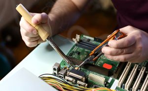
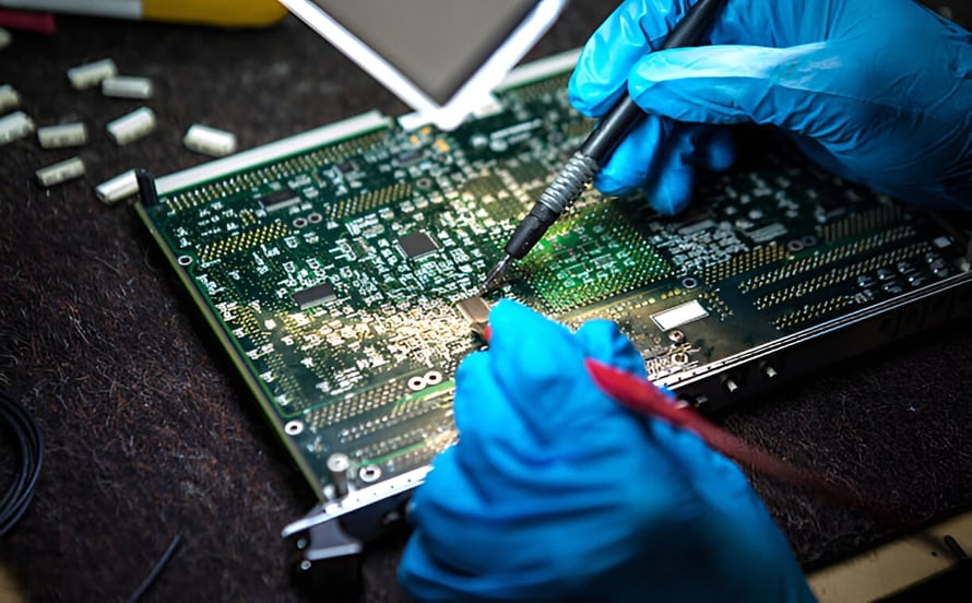
Having the right tools is essential for safe and controlled circuit board repair.
Common tools for basic PCB Repair include:
Soldering Iron
A temperature-controlled soldering iron is used to heat solder and create or rework electrical connections.
For delicate PCBs, temperature control is important because excessive heat can damage pads, traces, components, or the PCB laminate.
Desoldering Pump
A desoldering pump, sometimes called a solder sucker, removes molten solder from through-hole joints during component removal.
Solder Wire
Solder wire is used to create electrical and mechanical connections between components and PCB pads.
The solder alloy should be compatible with the PCB assembly and the applicable manufacturing requirements.
Flux
Flux helps remove surface oxides and improves solder wetting during soldering and rework.
The appropriate flux type should be selected according to the soldering process and component requirements.
Digital Multimeter
A digital multimeter (DMM) is one of the most useful tools for troubleshooting.
It can be used to measure:
- Voltage
- Resistance
- Continuity
- Diode forward voltage
- Capacitance on supported models
Tweezers
Fine-point ESD-safe tweezers are useful for handling small SMD components.
Magnifying Glass or Microscope
Magnification is especially useful for inspecting:
- Fine-pitch components
- Solder joints
- PCB traces
- Pads
- Vias
- Cracks
- Solder bridges
Small Screwdrivers and Plastic Pry Tools
These tools can help disassemble electronic equipment and access the PCB. Non-conductive pry tools are preferred where appropriate to reduce the risk of accidental electrical contact or mechanical damage.
Wire Cutters and Strippers
Small cutters can be used to trim through-hole component leads or repair wires. Wire strippers are useful when preparing jumper wires for trace repair.
Desoldering Braid
Desoldering braid, also called solder wick, is a copper braid used to remove excess solder from pads and connections.
Hot-Air Rework Station
A hot-air rework station can be used for removing and installing many SMD components, particularly components that are difficult to access with a conventional soldering iron.
PCB Repair Pen or UV-Curable Solder Mask
For certain trace or solder-mask repairs, specialized PCB repair materials can help restore insulation or protect repaired areas. The repair material should be compatible with the PCB and the intended application.
PCB Repair Safety Precautions
Safety should always come before attempting to repair a circuit board.
Disconnect Power
Always disconnect the equipment from its external power source before opening the enclosure or handling the PCB.
For battery-powered equipment, remove or disconnect the battery when the product’s service procedure allows it.
Important: Some equipment contains capacitors that can retain hazardous voltage even after the main power source has been disconnected. High-voltage power supplies, CRT equipment, mains-connected products, and similar systems should only be serviced by appropriately trained personnel.
Wear Eye Protection
Safety glasses can protect your eyes from solder splashes, clipped component leads, and small fragments.
Provide Adequate Ventilation
Soldering and rework can generate fumes. Work in a well-ventilated area and use appropriate local fume extraction.
Avoid deliberately inhaling soldering fumes.
Use ESD Protection
Sensitive semiconductor devices can be damaged by electrostatic discharge even when no visible damage occurs.
When appropriate, use:
- ESD wrist straps
- ESD mats
- Grounded workstations
- ESD-safe tools
- Appropriate component handling procedures
Avoid Working on Energized Circuits
Do not probe or solder a powered circuit unless the measurement or service procedure specifically requires energized testing and you are trained to perform it safely.
For beginners, de-energized troubleshooting is the safer approach.
PCB Repair Process: Step-by-Step Guide
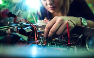
Once the basic tools and safety procedures are in place, you can follow a systematic process for basic circuit board troubleshooting and repair.
Step 1: Perform a Visual Inspection
The first step in almost every PCB Repair Process is a careful visual inspection.
Look for obvious signs of damage, including:
Burned or Discolored Areas
Darkened or discolored areas may indicate excessive temperature, an electrical overstress event, or component failure.
However, discoloration alone does not identify the root cause. Additional testing is normally required.
Broken or Lifted Traces
Mechanical damage, overheating, or previous repair work can cause traces to crack, break, or separate from the PCB surface.
Damaged Components
Look for:
- Bulging capacitors
- Cracked packages
- Burned resistors
- Broken connectors
- Melted plastic
- Discolored components
Some failed components, however, show no visible signs of damage.
Defective Solder Joints
Inspect solder joints for:
- Cracks
- Insufficient solder
- Solder bridges
- Poor wetting
- Lifted pads
- Mechanical damage
Use a microscope when working with fine-pitch or densely populated boards.
Step 2: Test the Circuit With a Multimeter
After visual inspection, electrical measurements can help narrow down the fault.
Continuity Testing
Continuity mode can help identify whether a trace or connection is electrically continuous.
A lack of continuity does not automatically mean that the PCB itself is defective; the circuit may intentionally contain a switch, resistor, semiconductor junction, or other element.
Resistance Testing
Measure resistance across appropriate circuit nodes and compare the result with the expected value.
Avoid measuring resistance on a powered circuit.
Testing Resistors
A resistor can be measured with the multimeter in resistance mode.
Compare the measured value with the nominal resistance and tolerance.
Keep in mind that measuring a resistor while it remains connected to other circuit paths may produce a reading different from its standalone value.
Testing Capacitors
Some multimeters provide capacitance measurement.
For accurate capacitor testing, the capacitor should generally be isolated from the circuit when necessary. A simple resistance or continuity test alone cannot fully determine whether a capacitor is healthy.
Testing Diodes and Transistors
The diode-test function can be useful for evaluating semiconductor junctions.
A healthy diode typically shows a forward voltage drop in one direction and a much higher resistance or out-of-range reading in the opposite direction.
For transistors, the expected readings depend on the transistor type and circuit configuration.
Step 3: Identify and Remove the Faulty Component
Once a defective component has been identified with sufficient confidence, it can be removed using an appropriate rework technique.
Heat the Solder Joint
Use a temperature-controlled soldering iron or an appropriate rework system to heat the solder joint.
Avoid prolonged heating.
Excessive thermal exposure can damage:
- Pads
- Traces
- Solder mask
- Components
- PCB laminate
Remove the Solder
For through-hole components, a desoldering pump or solder wick can be used to remove molten solder.
For SMD components, a soldering iron, hot-air station, or other suitable rework method may be used depending on the package.
Remove the Component
Once the solder connections have been sufficiently released, carefully remove the component.
Do not force a component from the PCB while solder remains solid because this can lift pads or damage through-hole plating.
Step 4: Install the Replacement Component
Before installing the replacement, verify that the new component matches the approved specification.
Check:
- Manufacturer part number
- Component value
- Package
- Voltage rating
- Current rating
- Tolerance
- Polarity
- Temperature rating
Then install the component according to the PCB layout and assembly requirements.
Solder the Component
Apply the appropriate amount of solder and heat the joint sufficiently to achieve proper wetting.
A good solder joint should be mechanically secure and electrically continuous without excessive solder, bridging, or obvious defects.
Trim Through-Hole Leads
For through-hole components, trim excess leads after soldering where appropriate.
Step 5: Repair Broken PCB Traces
If inspection identifies a broken trace, repairing the component alone will not restore the circuit.
A typical trace-repair process may include:
Clean the Repair Area
Clean the affected area using a suitable PCB-compatible cleaning method, such as isopropyl alcohol where appropriate.
Allow the area to dry completely.
Expose the Copper
Carefully remove a small amount of solder mask from the intact copper on both sides of the damaged trace.
The goal is to expose enough clean copper for the repair while minimizing additional damage.
Install a Jumper Wire
For suitable repair cases, a thin insulated wire can be used to bridge the damaged section.
The wire should be soldered to appropriate exposed copper areas on both sides of the break.
The repair wire should be routed so that it does not interfere with nearby components or create an unintended short.
Secure the Repair
After electrical verification, the jumper can be mechanically secured using an appropriate PCB-compatible adhesive or protective material when required.
For some applications, a UV-curable solder-mask repair material can be used to restore insulation and protect the repaired area.
For high-reliability products, trace repair should follow an approved repair procedure rather than an improvised jumper technique.
Step 6: Test the Repaired PCB
After completing the repair, do not immediately assume that the board is ready for use.
Perform appropriate verification.
Check for Shorts
Use a multimeter to check critical power rails and other relevant circuit nodes for unintended short circuits.
The expected resistance depends on the circuit, so a low resistance reading is not automatically evidence of a short.
Power Up Carefully
When the repair has passed the initial electrical checks, reconnect power using an appropriate and controlled test method.
For potentially damaged circuits, current-limited power supplies can help reduce the risk of additional damage.
Monitor for:
- Abnormal current consumption
- Excessive temperature
- Smoke or unusual odor
- Unexpected voltage levels
- Abnormal system behavior
Retest the Repaired Area
Verify that:
- The replacement component operates correctly.
- The repaired trace has continuity.
- No unintended connections exist.
- The original fault has been resolved.
- The PCB performs its intended function.
Functional testing should be based on the requirements of the specific product.
Step 7: Clean the PCB
After soldering and repair work, remove appropriate flux residues and debris when required.
A suitable PCB cleaning method should be selected according to the flux chemistry, component sensitivity, PCB materials, and manufacturer’s process requirements.
After cleaning, allow the board to dry completely before reassembly or energization.
Common PCB Repair Problems
Even experienced technicians can encounter difficulties during circuit board repair.
Lifted Pads
Excessive heat or mechanical force can cause a copper pad to separate from the PCB substrate.
This is particularly important when repairing fine-pitch or delicate boards.
Damaged Traces
Aggressive scraping or excessive heat can create additional trace damage.
Only expose the minimum amount of copper required for the repair.
Component Damage
Applying excessive heat to sensitive components can damage them even if the original problem was elsewhere.
Incorrect Replacement Components
A component with the same nominal value may not always be an appropriate replacement.
For example, replacing a capacitor requires consideration of voltage rating, capacitance, dielectric characteristics, package, temperature range, and other relevant parameters.
Hidden PCB Damage
Multilayer PCBs can contain internal damage that cannot be identified through a simple visual inspection.
More advanced methods such as X-ray inspection, electrical testing, or specialized failure analysis may be necessary.
PCB Repair vs PCB Rework
PCB repair and PCB rework are closely related but serve somewhat different purposes.
| Aspect | PCB Repair | PCB Rework |
|---|---|---|
| Primary purpose | Restore a defective or damaged board | Correct a manufacturing or assembly deviation |
| Typical example | Repair a broken trace | Replace an incorrectly installed component |
| Application | Field service, maintenance, production | Primarily manufacturing and engineering |
| Main objective | Restore required function | Bring the assembly into conformity |
| Documentation | Often required for traceability | Typically controlled through manufacturing procedures |
In practice, the terminology varies between organizations, and some manufacturers use “repair” and “rework” interchangeably.
When Should a PCB Be Repaired or Replaced?
Repair is not always the appropriate solution.
Before repairing a PCB, consider:
- Extent of damage
- Board construction
- Component availability
- Number of previous repairs
- Product safety requirements
- Reliability requirements
- Cost of repair
- Cost of replacement
- Expected remaining service life
For inexpensive consumer products, replacing the entire board may sometimes be more practical.
For expensive industrial, medical, automotive, aerospace, or specialized equipment, controlled repair may be economically and technically appropriate when permitted by the applicable requirements.
How PCB Design Can Improve Repairability
Repairability can be considered before manufacturing begins.
During PCB Design, engineers can improve serviceability by providing:
- Accessible test points
- Clear reference designators
- Appropriate component spacing
- Clearly marked polarity
- Modular circuit sections
- Suitable connector placement
- Adequate thermal clearance
- Diagnostic interfaces
Design-for-Test (DFT) and Design-for-Manufacturing (DFM) practices can also make troubleshooting and production support more efficient.
A repair-friendly PCB design can reduce the time required to locate and correct faults.
How PCB Manufacturing Affects Repair Requirements
The quality of PCB Manufacturing has a direct effect on the number and type of defects requiring repair.
Important manufacturing controls include:
- Material selection
- Controlled drilling
- Copper plating
- Etching
- Solder mask application
- Surface finishing
- Electrical testing
- Dimensional inspection
During PCB assembly, additional process controls are important for:
- Solder paste printing
- Component placement
- Reflow soldering
- Selective soldering
- AOI
- X-ray inspection
- Functional testing
Preventing defects at the manufacturing stage is generally preferable to relying heavily on downstream repair.
How Kingda Supports PCB Quality and Repair
Reliable PCB production requires coordination between design, fabrication, assembly, inspection, and testing.
At Kingda, manufacturing considerations can be incorporated into the PCB development process to help identify potential problems before they become production defects. Proper documentation, DFM review, inspection, testing, and controlled rework procedures can all contribute to consistent PCB quality.
When repair or rework is required, the objective should be to restore the board according to the applicable electrical, mechanical, and functional requirements rather than simply making the circuit operate temporarily.
For complex or high-reliability applications, repair procedures should be documented, controlled, and verified before the repaired assembly is released.
Final Summary
Learning how to repair a PCB starts with understanding the board’s structure, components, electrical connections, and common failure modes.
A basic PCB Repair Process typically includes:
Visual Inspection → Electrical Testing → Fault Identification → Component Removal → Component Replacement or Trace Repair → Inspection → Electrical Testing → Functional Verification → Cleaning
The right tools, including a temperature-controlled soldering iron, multimeter, desoldering equipment, tweezers, microscope, and suitable rework equipment, make the process more controlled and repeatable.
However, PCB repair should always be performed within the limits of the board, component, and product requirements. Simple repairs may be suitable for trained technicians or experienced electronics users, while mains-powered, high-voltage, safety-critical, multilayer, or highly complex assemblies may require specialized service personnel and documented repair procedures.
Ultimately, good PCB Design and reliable PCB Manufacturing are the first lines of defense against PCB failures. When repair is necessary, a systematic inspection, diagnosis, repair, and verification process can help restore the board while minimizing the risk of additional damage.