PCB Rework: PCB Design, PCB Manufacturing & Repair Process Guide
A printed circuit board (PCB) goes through numerous carefully controlled processes before becoming a finished product. From PCB Design and fabrication to component placement, soldering, inspection, and testing, every stage can introduce potential defects or deviations.
Although manufacturers implement quality-control measures to minimize defects, some issues may still occur during PCB Manufacturing and PCB assembly. Depending on the defect type and severity, the board may be repaired or reworked rather than discarded.
PCB Rework is an important manufacturing and quality-control activity used to correct specific defects, replace components, repair electrical connections, or make controlled modifications to a PCB. When properly performed, rework can recover otherwise usable boards, reduce material waste, and help maintain production schedules.
This article explains what PCB rework is, why it is important, how the PCB rework process works, and what challenges manufacturers need to consider.
What Is PCB Rework?
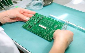
PCB rework refers to a controlled modification or corrective operation performed on a PCB or PCBA to correct a manufacturing or assembly defect, replace a defective component, or implement an approved modification.
Typical PCB rework operations include:
- Component removal and replacement
- Solder joint rework
- Solder bridge removal
- Broken trace repair
- Pad repair
- Via repair
- Wire modification
- Component relocation
- Adding or removing components
- Cutting an unintended connection
- Adding an approved jumper
- Correcting assembly defects
PCB rework should not be confused with uncontrolled modification. A proper rework operation follows an approved procedure and should preserve the intended electrical, mechanical, and functional characteristics of the assembly.
Rework can be required during prototype development, production, inspection, product qualification, or field service.
PCB Rework vs PCB Repair
Although the terms are often used interchangeably, there is a practical distinction.
PCB rework generally refers to modifying a PCB or PCBA to bring it into conformity with the approved design or manufacturing requirements.
PCB repair generally refers to restoring a defective or damaged board to functional condition.
For example:
- Replacing an incorrectly installed resistor can be considered rework.
- Removing a solder bridge can be considered rework.
- Repairing a broken PCB trace can be considered repair.
- Replacing a failed IC in a returned product can be considered repair.
In real manufacturing environments, the two activities can overlap, and manufacturers may use the terms according to their internal procedures.
Why Is PCB Rework Important?
PCB rework plays an important role in controlling production losses and maintaining product quality.
1. Reducing PCB Scrap
Not every defective PCB needs to be discarded.
If a defect is localized and technically repairable, reworking the board may allow the manufacturer to recover it.
This can reduce:
- PCB material waste
- Component waste
- Production losses
- Replacement manufacturing costs
- Disposal requirements
However, rework should only be performed when the resulting board can meet the applicable quality and reliability requirements.
2. Saving Production Time
Manufacturing an entirely new PCB assembly can take significantly longer than correcting a localized defect, especially when specialized components or fabricated boards have long lead times.
A controlled rework operation may allow a manufacturer to recover an assembly without restarting the entire production cycle.
3. Supporting Prototype Development
PCB rework is particularly useful during prototype development.
Engineering teams may discover that:
- A component value needs to be changed.
- A signal needs to be rerouted.
- A component needs to be relocated.
- An additional test point is required.
- A circuit requires a design modification.
Instead of manufacturing a completely new prototype for every minor change, controlled modifications may sometimes be used for engineering evaluation.
For production releases, however, recurring modifications should normally be incorporated into the formal PCB Design rather than relying on manual rework.
4. Correcting Assembly Defects
During PCB assembly, defects can occur in processes such as solder paste printing, component placement, and reflow soldering.
Examples include:
- Missing components
- Incorrect components
- Misaligned components
- Solder bridges
- Insufficient solder
- Excessive solder
- Poor solder joints
- Polarity errors
Appropriate rework procedures can correct certain defects before the product is released.
5. Supporting Field Service
PCB repair and rework may also be required after a product has been deployed.
A service center may replace a failed component or repair a localized connection instead of replacing the entire PCB assembly.
This can be particularly useful for products where the PCB is expensive, difficult to replace, or part of a long-term service program.
PCB Rework Process
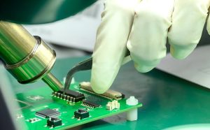
A professional PCB Rework process should be controlled and documented. The exact procedure depends on the PCB structure, component type, defect, materials, and applicable quality requirements.
Step 1: Identify the Defect
The first step is to determine what is wrong with the PCB.
Defect identification may involve:
- Visual inspection
- AOI results
- Electrical testing
- Functional testing
- X-ray inspection
- Microscopic inspection
- Thermal inspection
- Engineering analysis
The defect should be clearly documented before rework begins.
Step 2: Analyze the Failure
Once a defect is identified, engineers should determine its nature and, where practical, its root cause.
For example, a solder bridge may be caused by:
- Excessive solder paste
- Incorrect stencil design
- Component misalignment
- PCB pad design
- Printing-process variation
Simply removing the solder bridge may restore the board, but identifying the underlying process cause can help prevent the same defect from recurring.
Step 3: Determine Whether Rework Is Appropriate
Not every defective board should be reworked.
Before proceeding, consider:
- Defect severity
- Board construction
- Component accessibility
- Number of previous rework cycles
- Thermal sensitivity
- Pad and trace condition
- Product reliability requirements
- Cost of rework
- Cost of replacement
- Remaining product life
For high-reliability applications, the rework procedure may require additional engineering approval and inspection.
Step 4: Prepare the Rework Area
The rework workstation should be properly prepared before work begins.
Depending on the application, equipment may include:
- ESD-safe workstation
- Soldering station
- Hot-air rework system
- Preheater
- Microscope
- Desoldering equipment
- Flux and solder materials
- PCB fixtures
- Thermal monitoring equipment
- Inspection equipment
ESD protection is particularly important when handling sensitive semiconductor devices.
Step 5: Perform the Rework
The actual operation depends on the defect.
Common procedures include:
Component Replacement
The defective component is removed and replaced with the approved part.
The technician must verify:
- Correct part number
- Correct package
- Correct orientation
- Pad condition
- Soldering requirements
Solder Joint Rework
A defective solder joint can sometimes be reflowed or corrected using controlled soldering techniques.
Solder Bridge Removal
An unintended solder connection between adjacent pads can be removed using appropriate soldering and desoldering techniques.
Trace Repair
A damaged trace may be repaired using an approved conductive repair method. The repair must restore the required electrical connection while maintaining appropriate mechanical reliability.
Pad or Via Repair
Damaged pads and vias may require specialized repair techniques. These repairs are more complex than simple component replacement and should follow an appropriate repair procedure.
Step 6: Inspect the Reworked Area
After rework, the modified area should be inspected carefully.
Depending on the assembly, inspection may include:
- Visual inspection
- Microscopic inspection
- AOI
- X-ray
- Solder joint inspection
- Dimensional inspection
The purpose is to confirm that the rework itself has not introduced a new defect.
Step 7: Perform Electrical and Functional Testing
A reworked PCB should be tested according to the applicable product requirements.
Testing may include:
- Continuity testing
- Isolation testing
- Resistance measurement
- Voltage measurement
- ICT
- Functional testing
- Communication testing
- Power-up testing
The exact test method depends on the product and the nature of the rework.
Step 8: Document the Rework
The rework operation should be recorded for traceability.
Typical records may include:
- PCB serial number
- Defect description
- Defect location
- Rework method
- Replacement component
- Operator
- Date
- Inspection results
- Test results
- Engineering approval where required
These records can later be analyzed to identify recurring manufacturing or design problems.
Common PCB Rework Operations
| Rework Operation | Typical Purpose |
|---|---|
| Component replacement | Replace incorrect or defective components |
| Solder rework | Correct solder joint defects |
| Solder bridge removal | Eliminate unintended electrical connections |
| Trace repair | Restore damaged electrical paths |
| Pad repair | Restore damaged component attachment areas |
| Via repair | Restore electrical connections between layers |
| Jumper modification | Implement an approved circuit change |
| Component relocation | Correct placement or support engineering changes |
| Component removal | Remove an unnecessary or incorrect component |
The appropriate method depends on the PCB structure, component package, materials, and reliability requirements.
Challenges of PCB Rework
Although rework can reduce scrap and production losses, it introduces its own technical challenges.
1. Skilled Personnel
PCB rework should be performed by personnel with appropriate training and experience.
Technicians may need to understand:
- Circuit functionality
- Component identification
- Soldering techniques
- PCB construction
- ESD protection
- Thermal behavior
- Inspection methods
- Rework documentation
Insufficient training can cause additional damage, including lifted pads, overheated components, damaged solder mask, or broken traces.
2. Additional Equipment and Resources
Rework is usually performed outside the normal production sequence and may require dedicated equipment and personnel.
Depending on the application, manufacturers may need:
- Rework stations
- Microscopes
- Fixtures
- Specialized tools
- Testing equipment
- Replacement components
- Engineering support
These resources contribute to the overall rework cost.
3. Risk of Additional Damage
Repeated heating and mechanical manipulation can affect PCB materials and components.
Potential problems include:
- Lifted pads
- Damaged solder mask
- Delamination
- Component thermal damage
- Trace damage
- Via damage
- Reduced mechanical strength
Therefore, rework should use controlled thermal profiles and appropriate techniques rather than simply applying excessive heat.
4. High-Density PCB Complexity
Modern HDI and high-density PCB assemblies can be difficult to rework because components may be extremely small and closely spaced.
Fine-pitch packages, BGA devices, microvias, and densely routed boards can require specialized equipment and inspection techniques.
5. Component Availability
A rework operation cannot be completed efficiently if the required replacement component is unavailable.
This is why maintaining approved alternatives and accurate BOM information can be important for production continuity.
6. Time Constraints
Production schedules and customer delivery requirements can make rework time-critical.
The manufacturer must balance:
Rework Time + Labor + Material Cost + Testing Requirements
against the time and cost required to manufacture a replacement assembly.
7. Remaining Product Life
A repaired PCB may be returned to service, but rework does not automatically reset the aging history of the entire assembly.
For example, replacing one failed capacitor does not eliminate aging in the board’s other components, solder joints, connectors, or materials.
For products that have already experienced significant service exposure, engineers should consider the remaining expected service life before deciding whether rework is appropriate.
How to Improve PCB Rework Efficiency
PCB rework can be reduced by improving processes before defects occur.
Improve PCB Design
Good PCB Design practices can reduce manufacturing and assembly problems.
Designers should consider:
- DFM requirements
- DFT requirements
- Component accessibility
- Thermal management
- Appropriate pad geometry
- Assembly clearances
- Test-point accessibility
- Component availability
- Repairability
Designing for manufacturability and testability can reduce the need for corrective rework later.
Improve Manufacturing Process Control
Manufacturers should monitor critical fabrication and assembly processes.
For example:
- Stencil printing should be controlled.
- Component placement should be verified.
- Reflow profiles should be validated.
- AOI should identify assembly defects.
- Electrical testing should detect relevant faults.
- Process data should be analyzed for recurring defects.
A lower defect rate naturally reduces the amount of rework required.
Use Controlled Rework Procedures
Every recurring rework operation should have a documented procedure where appropriate.
The procedure can specify:
- Required equipment
- Materials
- Thermal limits
- Work sequence
- Inspection criteria
- Testing requirements
- Acceptance criteria
- Documentation requirements
This improves consistency between operators and production batches.
PCB Rework and Quality Control
PCB rework should be integrated into the broader quality-management system rather than treated as an isolated activity.
A typical quality loop is:
Defect Detection → Failure Analysis → Rework/Repair → Inspection → Testing → Documentation → Root-Cause Analysis → Process Improvement
This approach helps manufacturers use rework data to improve future production.
If the same defect repeatedly requires rework, the underlying cause should be investigated. It may indicate an issue with the PCB design, material selection, fabrication process, component sourcing, assembly process, or inspection method.
How Kingda Approaches PCB Rework
Reliable PCB Manufacturing depends not only on producing the board correctly the first time but also on having controlled procedures for handling defects when they occur.
At Kingda, PCB fabrication and assembly requirements can be evaluated together with inspection and testing requirements. When a rework operation is technically appropriate, the process should be controlled from defect identification through final verification.
The objective is to ensure that a reworked PCB meets the applicable electrical, mechanical, and functional requirements before it is released.
For production teams, effective rework management can help reduce unnecessary scrap, improve manufacturing efficiency, and provide useful data for continuous process improvement.
Final Summary
PCB Rework is an important part of modern PCB manufacturing and assembly. It allows manufacturers to correct certain defects, replace damaged components, repair electrical connections, and implement controlled engineering modifications without necessarily discarding the entire PCB assembly.
A reliable rework process should include defect identification, failure analysis, rework planning, controlled repair, inspection, electrical testing, functional verification, and documentation.
However, rework should not become a substitute for good manufacturing quality. Repeated defects should be investigated at their root cause so that improvements can be made to PCB Design, component selection, fabrication, assembly, and process control.
With appropriate procedures, trained personnel, suitable equipment, and effective quality management, PCB rework can be an important tool for reducing waste while maintaining the required quality and reliability of electronic products.