PCB Troubleshooting and Repair: PCB Design, PCB Manufacturing & Fault Diagnosis Guide
PCB failures are common problems that can affect almost any electronic device. As equipment ages, improper operation, manufacturing defects, environmental exposure, and electrical stress can gradually affect circuit performance and reliability. For engineers, technicians, and beginners, understanding PCB troubleshooting and repair is an important practical skill.
Finding the root cause of a PCB failure requires a systematic approach. Proper troubleshooting not only helps restore a defective circuit board but also provides valuable insight into component behavior, circuit operation, and potential weaknesses in the PCB manufacturing process. Engineers can use this practical knowledge when designing and developing new electronic circuits.
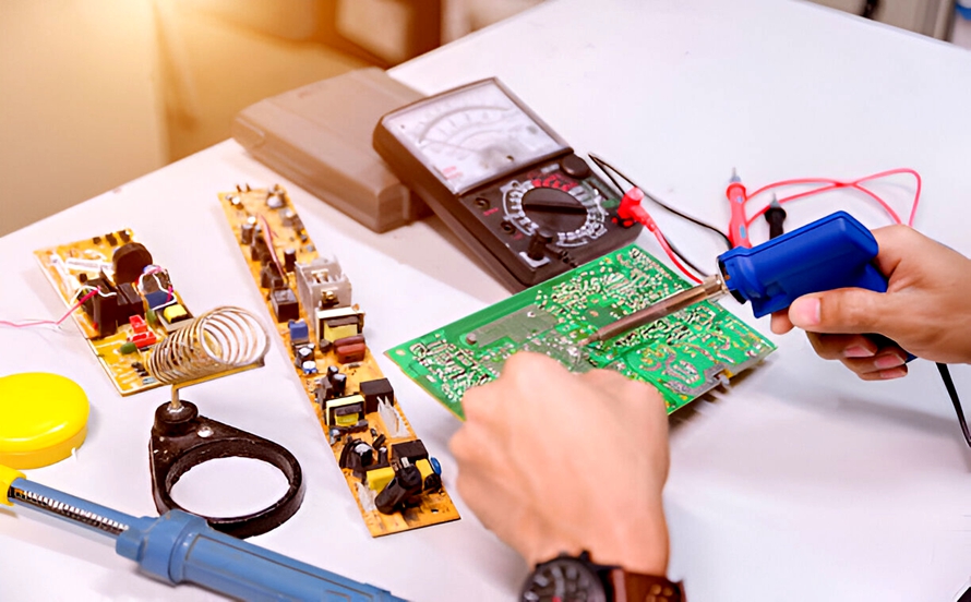
For simple circuit boards, basic laboratory equipment such as a digital multimeter, magnifying glass, oscilloscope, and soldering station may be sufficient. However, high-density multilayer boards and complex electronic assemblies often require more advanced inspection and automated test equipment.
This guide explains the major causes of PCB failures, the tools used for diagnosis, and a practical PCB repair workflow. It also discusses how PCB Design, PCB assembly, testing, and manufacturing quality can affect long-term reliability.
Why Do PCB Failures Occur?
Understanding the potential causes of circuit-board failure can significantly shorten the troubleshooting process. PCB diagnosis can involve multiple stages, so identifying likely failure mechanisms early helps engineers focus their testing on the most relevant areas.
Several factors can contribute to PCB failures, including physical damage, poor design, assembly defects, environmental contamination, and electrostatic discharge.
Physical Damage and Improper Handling
Electronic equipment may be exposed to impacts, vibration, accidental drops, mechanical stress, or mishandling during transportation, testing, installation, and maintenance.
These events can damage the PCB substrate, solder joints, components, connectors, or copper traces. A cracked board or damaged solder joint can create an open circuit, intermittent connection, or unintended electrical path.
For products exposed to vibration or mechanical shock, appropriate mechanical design and PCB mounting methods are essential for preventing premature failures.
Poor PCB Design
A reliable PCB begins with a well-engineered PCB Design.
Poor component placement, inadequate trace spacing, insufficient creepage distance, unsuitable trace widths, poor thermal management, and incomplete return paths can all contribute to reliability problems.
For example, traces carrying higher currents require appropriate width and copper thickness. High-voltage circuits also require sufficient clearance and creepage distances based on the applicable design requirements.
Thermal problems can occur when heat-generating components are placed too close together or when the PCB does not provide an adequate thermal path. Therefore, electrical, thermal, mechanical, and manufacturing considerations should all be addressed during PCB design.
PCB Assembly Problems
Incorrect assembly is another common source of PCB failure.
During PCB Assembly, components may be installed in the wrong location, orientation, polarity, or package position. Soldering defects can also create electrical or mechanical problems.
Typical assembly defects include:
- Solder bridges
- Insufficient solder
- Excessive solder
- Missing solder joints
- Cold or poorly formed solder joints
- Component polarity errors
- Misaligned components
- Tombstoning of passive components
- Lifted or damaged pads
Automated optical inspection (AOI), X-ray inspection, ICT, and functional testing can help identify these problems before defective assemblies reach the customer.
Environmental Factors
The operating environment has a significant influence on PCB reliability.
High humidity, condensation, dust, corrosive chemicals, salt contamination, extreme temperatures, and other environmental conditions can affect circuit boards over time.
Moisture combined with contaminants can promote corrosion or leakage currents. Conductive debris may create unintended electrical paths, while corrosive substances can damage copper conductors, solder joints, and component leads.
For harsh-environment applications, engineers may use conformal coatings, protective enclosures, appropriate surface finishes, and suitable PCB materials to improve reliability.
Electrostatic Discharge (ESD)
Electrostatic discharge can damage sensitive semiconductor devices even when there is no visible physical damage.
During PCB assembly, inspection, repair, or handling, an uncontrolled electrostatic discharge can transfer a high-voltage transient into sensitive components such as microcontrollers, memory devices, sensors, and communication ICs.
A proper ESD-controlled workstation should therefore be used when handling sensitive electronics. Grounded work surfaces, wrist straps, appropriate packaging, and controlled handling procedures can reduce ESD-related failures.
Essential Tools for PCB Fault Diagnosis
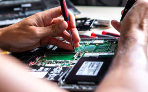
Simple single- or double-sided PCBs can often be diagnosed with basic laboratory equipment. More complex multilayer boards may require specialized inspection and automated test systems.
The following tools are commonly used for PCB troubleshooting.
1. Digital Multimeter (DMM)
A digital multimeter is one of the most important tools for PCB diagnosis.
Depending on the instrument and test conditions, a DMM can measure:
- DC and AC voltage
- Resistance
- Continuity
- Current
- Capacitance
- Diode forward voltage
Engineers can use these measurements to check power rails, fuses, resistors, diodes, connectors, and other accessible circuit nodes.
However, resistance and continuity measurements should normally be performed with the board unpowered. A continuity beep does not automatically indicate a short circuit because some PCB nets are intentionally connected or have naturally low resistance.
2. Digital Storage Oscilloscope (DSO)
An oscilloscope allows engineers to observe electrical waveforms rather than relying only on static voltage measurements.
A DSO can help analyze:
- Clock signals
- Communication signals
- Switching waveforms
- Reset signals
- PWM signals
- Analog waveforms
- Power-supply ripple
- Signal distortion
By comparing signals at different points in the circuit, engineers can identify where a signal becomes abnormal.
For difficult PCB troubleshooting, waveform comparison with a known-good board can be particularly useful.
3. Magnifying Equipment
A basic illuminated magnifier can reveal physical defects that are difficult to see with the naked eye.
For fine-pitch components and dense PCB layouts, a stereo microscope or digital inspection microscope can provide considerably better visibility.
Typical defects that can be identified include:
- Cracked solder joints
- Damaged pads
- Solder bridges
- Component damage
- Copper trace damage
- Contamination
- Board cracks
- Foreign material
4. Soldering and Rework Tools
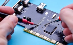
After identifying a defect, appropriate PCB rework equipment may be required.
Common tools include:
- Soldering iron
- Hot-air rework station
- Solder wick
- Desoldering pump
- Fine tweezers
- Flush cutters
- Solder wire
- Flux
- PCB holder
The appropriate tool depends on the component package and board construction. Excessive heat or mechanical force can damage multilayer boards, pads, vias, and nearby components.
5. Advanced Inspection and Test Equipment
Complex PCBs may require more sophisticated equipment, including:
- Automated optical inspection (AOI)
- X-ray inspection
- In-circuit testing (ICT)
- Functional circuit testing (FCT)
- Flying-probe testing
- Automated test equipment (ATE)
- Thermal imaging
- Boundary-scan testing
These systems are particularly useful for high-density multilayer PCBs where visual inspection and basic electrical measurements cannot reveal internal defects.
6. Design and Manufacturing Documentation
Technical documentation is just as important as physical test equipment.
Engineers should have access to relevant documents such as:
- Schematic diagrams
- PCB layout files
- Bill of materials (BOM)
- Assembly drawings
- Component datasheets
- Gerber or other fabrication data
- Test specifications
- Previous inspection reports
- Engineering change records
Having accurate documentation allows technicians to compare measured values with the intended circuit design.
Step-by-Step PCB Repair and Troubleshooting Process
A systematic troubleshooting workflow reduces unnecessary component replacement and helps engineers identify the actual root cause.
The following process can be adapted according to the PCB type, application, and reliability requirements.
1. Prepare the PCB Repair Workstation
Start by preparing a clean, well-lit, ESD-controlled workstation.
Recommended equipment includes:
- ESD workbench
- ESD wrist strap
- PCB holder
- Magnification equipment
- Digital multimeter
- Oscilloscope
- Soldering equipment
- Proper ventilation or fume extraction
Before testing, disconnect the PCB from its power source and external equipment whenever practical.
For high-voltage, mains-powered, or energy-storage circuits, additional safety procedures are required. Capacitors can retain hazardous energy even after the main power source has been disconnected.
2. Perform a Thorough Visual Inspection
Visual inspection should normally be the first diagnostic step.
Look for:
- Burn marks
- Discolored PCB areas
- Damaged components
- Cracked packages
- Incorrect component orientation
- Solder bridges
- Missing solder
- Poor solder joints
- Lifted pads
- Broken traces
- Cracked PCB material
- Damaged connectors
- Corrosion
- Contamination
- Unusual hot spots
Thermal imaging can be useful when a component is overheating but does not show obvious physical damage.
3. Compare the Failed PCB with a Known-Good Board
If a functional reference board is available, comparison can greatly accelerate troubleshooting.
Engineers can compare:
- Component placement
- Component markings
- Power-rail voltages
- Resistance measurements
- Signal waveforms
- Connector pin voltages
- IC input and output signals
- Temperature distribution
A known-good board provides a practical reference for distinguishing normal circuit behavior from abnormal behavior.
However, boards should only be compared when they have the same revision, configuration, and operating conditions. Otherwise, differences may be intentional.
4. Check for Shorts and Abnormal Resistance
With the PCB unpowered, use a multimeter to check important power rails and ground connections.
If an unusually low resistance is measured between a power rail and ground, further investigation may be necessary. However, low resistance alone does not prove that a short circuit exists because some power circuits naturally have low DC resistance.
Technicians can isolate sections of the circuit and inspect components such as:
- Capacitors
- Diodes
- Transistors
- ICs
- Resistors
- Inductors
- Voltage regulators
Component measurements should be interpreted according to the circuit topology and manufacturer specifications rather than relying on a single generic resistance value.
5. Power Up the PCB Carefully
After completing the initial unpowered checks, the board can be powered under controlled conditions when appropriate.
If possible, use a current-limited laboratory power supply. Monitor:
- Input current
- Main supply voltage
- Secondary power rails
- Regulator outputs
- Temperature
- Startup behavior
Unexpected zero voltage, excessive current consumption, unstable voltage, or abnormal heating can indicate a problem in the corresponding circuit section.
For valuable or safety-critical boards, avoid repeatedly powering a suspected defective circuit without understanding the possible fault mechanism.
6. Trace the Fault Through the Circuit
Use the schematic to divide the PCB into functional blocks.
For example:
Power Input → Protection → Regulation → Processing → Communication → Output
Testing each block systematically can help identify where normal operation stops.
An oscilloscope is particularly useful for checking signals before and after suspected components. Comparing input and output waveforms can reveal whether a component or circuit stage is causing signal degradation.
7. Repair Broken Traces or Pads
A damaged copper trace can interrupt the electrical connection between two circuit nodes.
Depending on the damage and reliability requirements, a controlled repair may involve:
- Cleaning the damaged area.
- Exposing a suitable amount of intact copper if necessary.
- Applying appropriate flux.
- Installing a small jumper wire or approved repair material.
- Soldering the connection carefully.
- Providing mechanical support where required.
- Verifying electrical continuity.
For small, localized trace damage, solder reinforcement may sometimes be sufficient. For high-current or high-frequency circuits, however, the repair must preserve the required electrical characteristics.
Pad and via damage is more complicated and may require specialized PCB repair techniques.
8. Verify Suspected Integrated Circuits
Modern PCBs contain many integrated circuits, including:
- Microcontrollers
- DC-DC converters
- Memory devices
- Analog sensors
- Digital sensors
- Isolation ICs
- Communication controllers
- CAN transceivers
- Power-management ICs
Identifying a failed IC can be more difficult than identifying a visibly damaged component.
Engineers can use the schematic and datasheet to verify:
- Supply voltage
- Enable signals
- Reset signals
- Clock signals
- Input signals
- Output signals
- Communication activity
Oscilloscope measurements can help determine whether an IC is receiving the correct inputs and producing the expected outputs.
A known-good board is especially valuable for waveform comparison.
9. Use Automated Testing for Complex PCBs
Automated test equipment can significantly improve the efficiency and repeatability of PCB testing.
For complex multilayer boards, common methods include:
In-Circuit Testing (ICT)
ICT checks specific nodes and components through a test fixture or other dedicated test interface. It can identify many manufacturing-related electrical faults.
Functional Circuit Testing (FCT)
FCT evaluates whether the assembled PCB performs its intended functional operations under defined test conditions.
Flying-Probe Testing
Flying-probe systems use movable probes to test electrical connections without requiring a dedicated fixture, making them useful for certain prototype and low-volume applications.
Automated Test Equipment (ATE)
ATE can combine electrical measurements, functional tests, and software-controlled analysis to improve testing consistency.
The appropriate system depends on PCB complexity, production volume, test coverage, product requirements, and available test access.
Common PCB Repair Problems and Recommended Responses
| PCB Problem | Possible Cause | Typical Diagnostic Approach |
|---|---|---|
| No power | Open connection, fuse, protection device, regulator failure | Check input voltage, current, fuse, and power rails |
| Excessive current | Shorted component or damaged IC | Use current-limited power and isolate circuit sections |
| Intermittent operation | Cracked solder joint, connector, trace, or mechanical stress | Visual inspection, mechanical inspection, waveform testing |
| Overheating | Excessive current, poor thermal path, failed component | Thermal inspection and current/voltage measurements |
| No communication | IC failure, missing clock, incorrect supply, damaged interface | Check power, clock, TX/RX or bus signals |
| Open circuit | Broken trace, via, solder joint, connector | Continuity testing and visual inspection |
| Unexpected reset | Power instability, reset circuit fault, firmware-related issue | Monitor supply and reset signals |
| Signal distortion | Layout issue, damaged component, impedance discontinuity, noise | Oscilloscope and signal-integrity analysis |
PCB Repair vs. PCB Rework
Although PCB repair and PCB rework are closely related, they are not exactly the same.
PCB rework generally refers to modifying an assembled PCB to correct a manufacturing or assembly issue, such as replacing an incorrectly installed component.
PCB repair generally refers to restoring a board that has suffered electrical, mechanical, thermal, or environmental damage.
Examples include:
- Replacing a wrongly installed resistor → PCB rework
- Replacing a defective IC → May be rework or repair depending on the situation
- Repairing a broken copper trace → PCB repair
- Repairing a damaged pad → PCB repair
- Correcting a solder bridge → PCB rework
The distinction is useful because repair and rework may require different procedures, documentation, acceptance criteria, and reliability evaluations.
How PCB Design and Manufacturing Affect Reliability
Many PCB failures can be traced back to issues that originated before the board was ever repaired.
During PCB Design, engineers should consider:
- Trace width and current capacity
- Clearance and creepage
- Thermal management
- Component derating
- Signal integrity
- Power integrity
- Return-current paths
- Mechanical stress
- Connector reliability
- ESD protection
- Test-point accessibility
- Design for manufacturability (DFM)
- Design for testability (DFT)
During PCB Manufacturing, process control is equally important.
Manufacturers should control:
- Lamination quality
- Drilling accuracy
- Plating thickness
- Solder mask quality
- Surface finish
- Soldering quality
- Component placement
- Electrical testing
- AOI inspection
- X-ray inspection where appropriate
A well-designed PCB can still fail if manufacturing quality is inconsistent. Conversely, a high-quality manufacturing process cannot compensate for fundamental design problems.
Best Practices for Preventing Repeated PCB Failures
Repairing a failed PCB is only part of the solution. Engineers should also determine why the failure occurred and whether the same mechanism could affect other units.
Recommended practices include:
- Identify the root cause rather than replacing components randomly.
- Record all diagnostic measurements before and after repair.
- Use current-limited power supplies when powering a suspected defective board.
- Follow ESD protection procedures during assembly and repair.
- Use the latest schematic, BOM, and PCB revision.
- Compare failed boards with verified-good units when available.
- Inspect repaired areas under magnification.
- Perform electrical and functional testing after repair.
- Document component substitutions and repair modifications.
- Analyze recurring failures at the design and manufacturing levels.
For high-reliability applications, repair procedures should follow the product’s approved engineering and quality requirements rather than relying solely on general laboratory practices.
Cost Considerations in PCB Repair
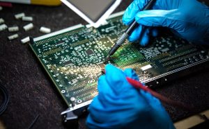
Repair is not always economically or technically preferable to replacing a PCB.
Engineers and manufacturers should consider:
- PCB replacement cost
- Component cost
- Labor cost
- Diagnostic time
- Specialized equipment requirements
- Previous repair history
- Board complexity
- Remaining product life
- Reliability requirements
- Risk of additional damage during repair
For expensive multilayer boards or assemblies containing high-value components, repair may reduce material waste and replacement costs. However, the final decision should also account for reliability and warranty requirements.
If an EMI shield or conductive enclosure has been mechanically damaged, the appropriate repair method depends on its construction and electrical requirements. Conductive coatings may be suitable for certain applications, but the repaired shield should be verified for electrical continuity and shielding performance.
Conclusion
PCB failures can result from many different factors, including physical damage, poor PCB Design, assembly defects, environmental contamination, ESD, component aging, and manufacturing problems.
Effective PCB troubleshooting requires a systematic process rather than random component replacement. Engineers should begin with documentation and visual inspection, followed by unpowered electrical checks, controlled power-up, signal analysis, component testing, and functional verification.
Basic tools such as a digital multimeter, oscilloscope, microscope, and soldering equipment are sufficient for many simple repairs. More complex multilayer boards may require AOI, X-ray inspection, ICT, FCT, flying-probe testing, or other automated test systems.
Most importantly, PCB repair should not stop at restoring functionality. Repeated failures should be analyzed at the PCB Design, assembly, and PCB Manufacturing levels to identify and eliminate the underlying causes.
With a structured diagnostic workflow, appropriate test equipment, accurate technical documentation, and controlled repair procedures, engineers can improve PCB reliability while reducing unnecessary component replacement and production downtime.
Kingda: Professional PCB Design and Manufacturing Support
Kingda provides PCB solutions covering PCB Design, fabrication, assembly, testing, and related engineering support. By combining design-for-manufacturing principles with controlled production and inspection processes, Kingda helps customers develop reliable circuit boards for demanding electronic applications.
For engineers and purchasing teams, selecting a PCB manufacturing partner with appropriate technical capabilities, quality controls, testing resources, and engineering support is an important part of building a reliable electronics supply chain.