1 oz Copper PCB Thickness: PCB Design, PCB Manufacturing & Copper Weight Guide
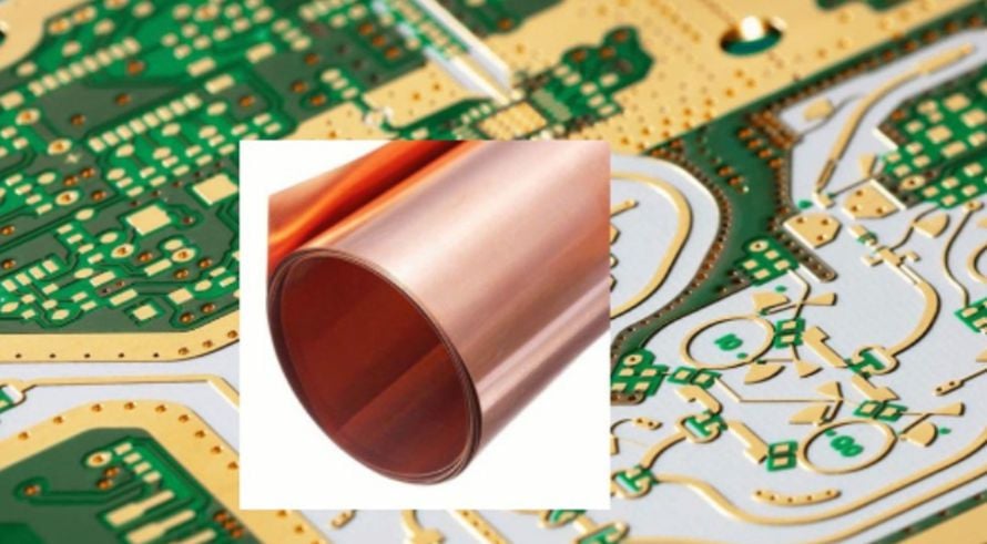
A printed circuit board (PCB) is constructed from multiple layers of conductive and dielectric materials. Among these layers, copper is one of the most important because it forms the electrical pathways that connect components and distribute power and ground throughout the board.
Copper is used for signal traces, power planes, ground planes, thermal areas, pads, vias, and plated holes. Therefore, copper thickness is an important parameter in both PCB Design and PCB Manufacturing.
One of the most common copper specifications used in PCB fabrication is 1 oz copper. Engineers frequently encounter this specification in PCB quotations, fabrication drawings, and stackup documentation. However, “1 oz” describes copper weight rather than directly describing thickness.
Understanding the relationship between copper weight and thickness helps engineers select appropriate materials, calculate current-carrying capacity, control impedance, evaluate thermal performance, and communicate accurately with PCB manufacturers.
This guide explains what 1 oz copper means, its advantages and limitations, how it compares with 2 oz and 3 oz copper, and how copper distribution affects advanced PCB manufacturing.
What Is the Thickness of 1 oz Copper?
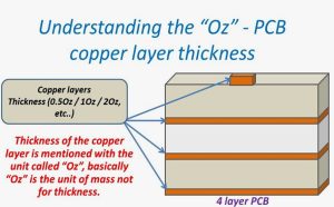
In PCB manufacturing, copper thickness is commonly specified by copper weight.
One ounce (1 oz) of copper means that one avoirdupois ounce of copper is distributed uniformly over an area of one square foot.
Therefore:
1 oz copper = 28.35 g/ft²
The theoretical thickness can be calculated using the density of copper, which is approximately 8.96 g/cm³.
Since:
1 ft² ≈ 929 cm²
The volume of 28.35 g of copper is approximately:
Volume = Mass ÷ Density
Volume ≈ 28.35 ÷ 8.96 ≈ 3.16 cm³
The corresponding thickness is:
Thickness = Volume ÷ Area
Thickness ≈ 3.16 ÷ 929 ≈ 0.0034 cm
This gives a theoretical copper thickness of approximately:
34 µm, commonly rounded to 35 µm
In imperial units:
1 oz copper ≈ 1.37 mil
Therefore, a commonly used PCB industry conversion is:
| Copper Weight | Nominal Copper Thickness |
|---|---|
| 0.5 oz | ~17 µm |
| 1 oz | ~35 µm |
| 2 oz | ~70 µm |
| 3 oz | ~105 µm |
| 4 oz | ~140 µm |
These values are nominal. Actual copper thickness in a finished PCB can vary because of the starting foil thickness, plating, etching, manufacturing tolerances, and whether the specification refers to base copper or finished copper.
Why Is 1 oz Copper So Widely Used?
1 oz copper has become a common starting point for many PCB applications because it provides a practical balance between electrical performance, manufacturability, cost, and routing density.
However, 1 oz copper should not automatically be considered the default for every PCB. The appropriate copper thickness depends on current requirements, thermal performance, mechanical constraints, signal characteristics, manufacturing capability, and applicable design standards.
Broad Application Range
1 oz copper is widely used in many types of electronics, including:
- Consumer electronics
- Industrial controls
- Telecommunications
- Automotive electronics
- Computing equipment
- IoT devices
- Instrumentation
- General-purpose control boards
More specialized applications may require thinner or thicker copper depending on their electrical and mechanical requirements.
Good Electrical Conductivity
Copper has high electrical conductivity, which makes it well suited for PCB traces and planes.
With appropriate trace width and copper thickness, 1 oz copper can support a wide range of low- and moderate-current circuits.
However, current-carrying capability is not determined by copper weight alone. Engineers should also consider trace width, allowable temperature rise, ambient conditions, copper geometry, and whether the conductor is on an external or internal layer.
Thermal Performance
Copper also helps distribute and remove heat.
Large copper areas can spread heat away from power components, while thermal vias can transfer heat between PCB layers or toward a thermal management structure.
For higher-power applications, however, increasing copper thickness may be only one part of the thermal solution. Component placement, copper area, thermal vias, heat sinks, airflow, and PCB material all influence thermal performance.
Mechanical and Manufacturing Balance
1 oz copper provides a useful balance between conductor thickness and manufacturing complexity.
Very thick copper can require specialized etching and plating processes and may impose additional limitations on fine-line routing.
Therefore, standard copper thickness is often preferred when the electrical requirements do not justify heavier copper.
Good Solderability
Copper forms the conductive foundation beneath PCB pads and other plated structures. Properly manufactured and finished copper surfaces can provide reliable soldering performance.
It is important to note that solderability is primarily determined by the PCB surface finish, pad design, cleanliness, and assembly process rather than by copper thickness alone.
Cost Efficiency
Using unnecessarily thick copper can increase material and manufacturing costs.
If the electrical requirements can be met with 1 oz copper, there may be little reason to use 2 oz, 3 oz, or heavier copper purely for the sake of increasing thickness.
For this reason, 1 oz copper is a practical option for many standard PCB designs.
When Should You Use Thicker Copper?
Although 1 oz copper is suitable for many designs, certain applications require heavy copper PCB construction.
Common reasons for increasing copper thickness include:
- Higher current capacity
- Lower conductor resistance
- Reduced voltage drop
- Improved heat spreading
- Higher power density
- Increased conductor robustness
- Power electronics requirements
Typical heavy-copper configurations include 2 oz, 3 oz, 4 oz, and even higher copper weights.
For example, a power distribution PCB carrying substantial current may require wider and thicker copper conductors to maintain acceptable temperature rise and voltage drop.
However, simply increasing copper thickness does not automatically improve every aspect of PCB performance.
Disadvantages of Using Thicker Copper
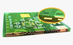
Using 2 oz, 3 oz, or heavier copper can introduce additional design and manufacturing challenges.
Reduced Fine-Line Capability
Thicker copper is generally more difficult to etch precisely.
During etching, the copper profile can develop undercutting, which affects trace width and spacing. As copper becomes thicker, maintaining very fine geometries can become more challenging.
Therefore, heavy copper and ultra-fine-pitch routing may require careful process selection and design rules.
Increased Manufacturing Complexity
Thick copper may require adjustments to:
- Etching parameters
- Plating processes
- Lamination structures
- Drill processes
- Solder mask processing
- Surface finishing
- Inspection procedures
Manufacturers must establish appropriate process windows for the selected copper thickness.
Larger PCB Area Requirements
Heavy copper designs may require wider traces and larger clearances depending on the electrical requirements.
This can consume more routing space and potentially increase PCB dimensions.
More Difficult Soldering and Thermal Control
Thick copper areas can absorb and distribute heat during soldering.
Large copper planes connected to component pads may therefore affect thermal balance during assembly and rework.
The assembly process may need appropriate thermal profiling to ensure reliable solder joints.
Higher Cost
More copper material and more demanding manufacturing processes can increase PCB fabrication costs.
Therefore, copper thickness should be selected based on actual electrical and thermal requirements rather than simply choosing the thickest available option.
1 oz vs. 2 oz vs. 3 oz Copper
The following table provides a practical comparison.
| Characteristic | 1 oz Copper | 2 oz Copper | 3 oz Copper |
|---|---|---|---|
| Nominal thickness | ~35 µm | ~70 µm | ~105 µm |
| Typical use | General-purpose PCBs | Higher-current designs | Heavy-current/power applications |
| Current capacity | Moderate, depending on trace width | Higher | Higher still |
| Resistance | Higher than heavier copper for the same geometry | Lower | Lower |
| Voltage drop | Depends on trace geometry | Reduced for equivalent geometry | Further reduced |
| Fine-line routing | Generally easier | More challenging | More challenging |
| Manufacturing complexity | Standard | Increased | Higher |
| Material/process cost | Lower | Higher | Higher |
| Thermal spreading | Good with sufficient copper area | Improved conductor cross-section | Higher conductor cross-section |
| Board-space efficiency | Often favorable | May require wider traces | May require more routing space |
The exact current-carrying capability should be calculated using the applicable design methodology rather than inferred solely from copper weight.
Copper Thickness and PCB Current-Carrying Capacity
One of the most important reasons for selecting thicker copper is to increase conductor cross-sectional area.
For a simplified conductor:
Resistance = Resistivity × Length ÷ Cross-sectional Area
Increasing copper thickness increases the conductor cross-sectional area when trace width remains constant. This can reduce resistance and voltage drop.
At the same time, higher current generates more heat.
Therefore, PCB Design should consider the relationship between:
- Copper thickness
- Trace width
- Trace length
- Current
- Temperature rise
- Ambient temperature
- Copper layer location
- Thermal dissipation
IPC-based design methods can be used to estimate allowable conductor temperature rise and current-carrying capacity.
Engineers should also consider the complete power-delivery path rather than evaluating a single trace in isolation.
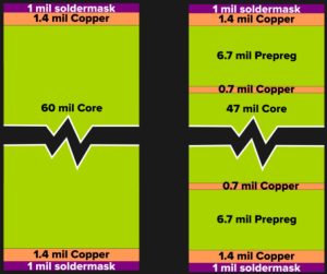
Copper Layer Arrangement in PCB Stackup
Copper thickness is only one part of the overall PCB stackup.
In multilayer PCBs, engineers must carefully determine how signal, power, and ground layers are arranged.
A typical multilayer PCB may contain:
- Signal layers
- Ground planes
- Power planes
- Mixed signal/power layers
A well-designed stackup helps provide continuous signal return paths, controlled impedance, effective power distribution, and manageable electromagnetic interference.
For high-speed circuits, the distance between signal and reference planes can be just as important as the copper thickness itself.
Copper Symmetry
Balanced copper distribution is important during multilayer PCB fabrication.
If one region contains significantly more copper than another, differences in resin flow, thermal expansion, and mechanical stress can contribute to board deformation or other manufacturing challenges.
Engineers should therefore consider copper balance across the PCB stackup.
Why Uneven Copper Distribution Can Cause Problems
Copper distribution affects both PCB Manufacturing and final board reliability.
1. Resin Flow and Lamination Effects
During multilayer lamination, dielectric materials flow around copper structures.
Large differences in copper density can affect resin distribution and local dielectric thickness.
Appropriate copper balancing and stackup planning help maintain more consistent lamination results.
2. Board Bow and Twist
Uneven copper distribution can contribute to mechanical deformation such as board bow and twist.
This is particularly important for large multilayer PCBs and assemblies with tight dimensional requirements.
Board deformation can affect:
- SMT placement
- Reflow soldering
- Connector alignment
- Mechanical assembly
- Final enclosure fit
3. Uneven Thermal Distribution
Copper has high thermal conductivity.
Large differences in copper density can therefore create differences in local thermal behavior during fabrication and operation.
Thermal analysis is especially important for high-power PCBs.
4. Manufacturing Yield
Unbalanced copper distribution can make etching and plating more difficult to control.
Designers should work with the PCB manufacturer to ensure that copper density, trace geometry, plating requirements, and manufacturing tolerances are compatible with the fabrication process.
Copper Etching and Thickness Control
Copper thickness directly affects the etching process.
During PCB fabrication, unwanted copper is removed to create the required circuit pattern.
As copper becomes thicker, controlling:
- Etch rate
- Undercut
- Trace width
- Trace spacing
- Copper profile
becomes increasingly important.
For fine-line designs, engineers should not assume that a layout created using thin copper can automatically be manufactured using significantly thicker copper.
The PCB manufacturer should confirm the applicable design rules before production.
Base Copper vs. Finished Copper
An important consideration when specifying copper thickness is whether the value refers to base copper or finished copper.
Base Copper
Base copper is the copper foil supplied before additional manufacturing processes such as pattern plating.
Finished Copper
Finished copper refers to the copper thickness after relevant PCB fabrication processes have been completed.
The final copper thickness can therefore differ from the nominal starting foil thickness.
This distinction is especially important when specifying:
- Outer-layer copper
- Inner-layer copper
- Plated holes
- Heavy copper
- High-current traces
When requesting a quotation, engineers should clearly define the copper specification they require.
How Copper Thickness Affects PCB Design
Copper weight should be considered early in the design process because it can affect multiple aspects of the PCB.
Trace Width
Higher-current traces may require greater width, greater copper thickness, or both.
Impedance Control
For controlled-impedance circuits, trace width, copper thickness, dielectric thickness, dielectric constant, and reference-plane geometry interact with one another.
Changing copper thickness after the PCB layout has been completed can therefore affect impedance calculations.
Thermal Design
Copper thickness and copper area influence heat spreading.
Power components may require large copper areas and thermal vias in addition to thicker copper.
Manufacturing Rules
Thick copper can affect minimum trace width, minimum spacing, etching capability, plating, and other fabrication parameters.
Therefore, copper weight should be included in the PCB fabrication specification before final design release.
Practical Copper Thickness Selection Guide
Engineers can use the following general approach when selecting copper thickness:
Choose 1 oz Copper When:
- The PCB carries low to moderate current.
- Standard routing density is required.
- Fine-line routing is important.
- Cost efficiency is a priority.
- Standard PCB fabrication processes are preferred.
Consider 2 oz Copper When:
- Current requirements are higher.
- Lower voltage drop is required.
- Additional thermal spreading is beneficial.
- Power traces occupy limited board area.
- The design can accommodate heavier copper manufacturing rules.
Consider 3 oz or Heavier Copper When:
- High-current power distribution is required.
- Significant conductor heating must be controlled.
- Heavy-copper construction is part of the application requirements.
- The PCB is used for power conversion, energy systems, industrial equipment, or other high-current applications.
The final selection should always be based on calculated electrical and thermal requirements and confirmed with the PCB manufacturer.
Common Misconceptions About 1 oz Copper
1 oz Does Not Mean the PCB Is 1 oz Thick
The “1 oz” specification applies to the copper layer, not the total PCB thickness.
A PCB can contain 1 oz copper while having an overall board thickness of 0.8 mm, 1.0 mm, 1.6 mm, 2.0 mm, or another specified thickness.
1 oz Does Not Automatically Mean 35 µm Finished Copper
Approximately 35 µm is the theoretical nominal thickness corresponding to 1 oz of copper uniformly distributed over one square foot.
Actual finished copper depends on the manufacturer’s process and the specification being referenced.
Thicker Copper Does Not Automatically Mean Better PCB Performance
A thicker copper layer can improve current capacity and reduce resistance under appropriate conditions, but it may also increase cost and manufacturing difficulty.
PCB performance depends on the complete design rather than copper thickness alone.
Conclusion
1 oz copper is one of the most widely used copper specifications in PCB manufacturing because it provides a practical balance among electrical performance, routing capability, manufacturing complexity, and cost.
The theoretical thickness of 1 oz copper is approximately 35 µm or 1.37 mil. However, engineers should distinguish between copper weight, base copper thickness, and finished copper thickness when communicating PCB requirements with manufacturers.
For higher-current and power-intensive applications, 2 oz, 3 oz, or heavier copper may be appropriate. These options can reduce conductor resistance, lower voltage drop, increase current-carrying capability, and improve heat spreading. At the same time, thicker copper can make fine-line etching, plating, lamination, soldering, and overall manufacturing more challenging.
Copper distribution across the PCB is also important. Balanced copper density, appropriate stackup design, controlled impedance, adequate thermal management, and manufacturable trace geometries all contribute to a reliable board.
Ultimately, the correct copper thickness should be determined by the electrical, thermal, mechanical, and manufacturing requirements of the application. By integrating copper selection into PCB Design and PCB Manufacturing from the beginning, engineers can avoid unnecessary redesigns and achieve a more reliable and manufacturable PCB.
Kingda PCB Manufacturing Support
Kingda provides PCB fabrication and assembly solutions for projects requiring different copper thicknesses and PCB structures.
For standard electronics as well as higher-current applications, copper weight can be evaluated together with PCB layer count, stackup, trace width, thermal requirements, surface finish, impedance requirements, and assembly specifications.
Early communication between the design team and manufacturer helps ensure that the selected copper thickness can be produced within the required manufacturing tolerances.